 Products Home
Germanium Windows
- Offered Uncoated or with AR Coating for 1.9 - 6 µm or 7 - 12 µm
- Ø1/2" and Ø1" Sizes Available
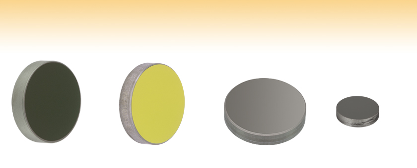
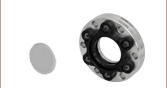
WG91050-E3
Ø1"
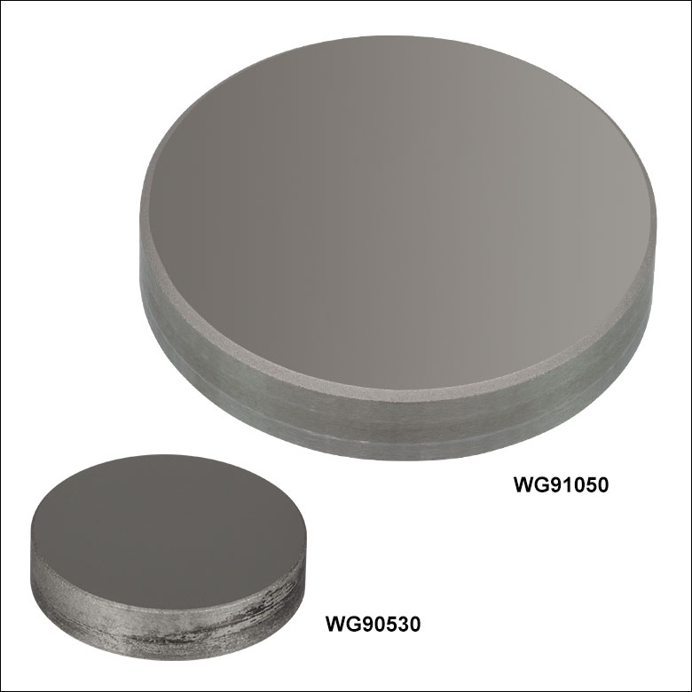
WG91050
Ø1"
WG90530
Ø1/2"
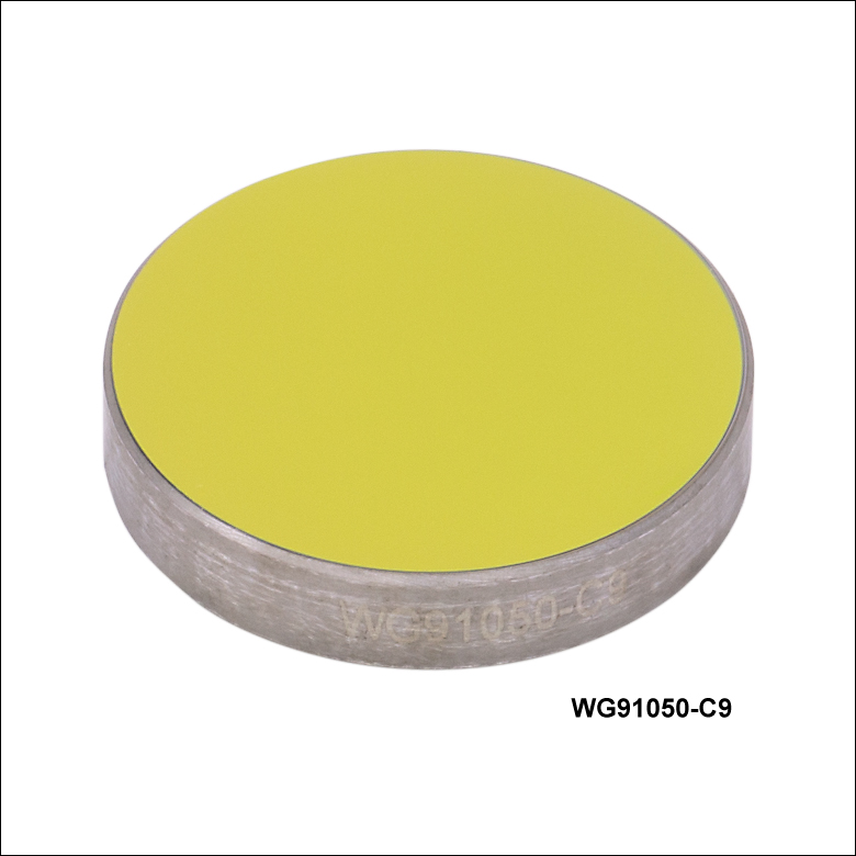
WG91050-C9
Ø1"


Please Wait
| Flat Window Selection Guide | |
|---|---|
| Wavelength Range | Substrate Material |
| 180 nm - 8.0 μm | Calcium Fluoride (CaF2) |
| 185 nm - 2.1 μm | UV Fused Silica |
| 200 nm - 5.0 μm | Sapphire |
| 200 nm - 6.0 μm | Magnesium Fluoride (MgF2) |
| 220 nm to >50 µm | CVD Diamond Windows |
| 230 nm - 1.1 µm | UV Fused Silica, Textured Antireflective Surface |
| 250 nm - 1.6 µm | UV Fused Silica, for 45° AOI |
| 250 nm - 26 µm | Potassium Bromide (KBr) |
| 300 nm - 3 µm | Infrasil® |
| 350 nm - 2.0 μm | N-BK7 |
| 600 nm - 16 µm | Zinc Selenide (ZnSe) |
| 1 - 1.7 µm | Infrasil®, Textured Antireflective Surface |
| 1.2 - 8.0 μm | Silicon (Si) |
| 1.9 - 16 μm | Germanium (Ge) |
| 2 - 5 μm | Barium Fluoride (BaF2) |
| V-Coated Laser Windows | |
Features
- 1/2" and 1" Diameters Available
- Useful for IR Applications in the 1.9 - 16 µm Spectral Range
- Available Uncoated or with One of Two AR Coatings:
- 1.9 to 6 µm (-C9): <2% Average Reflectance
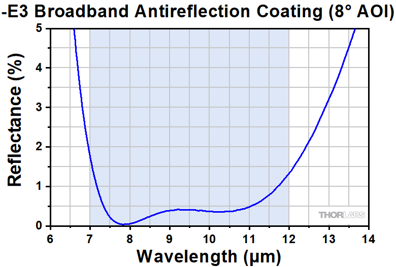
- 7 to 12 µm (-E3): <1% Average Reflectance
- Ideal Longpass Filter for Above 2 µm (See Graphs Tab)
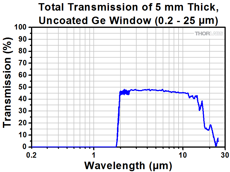
Thorlabs' Precision Germanium (Ge) Windows are offered in Ø1/2" and Ø1" sizes. The uncoated versions are transmissive at wavelengths from 2 to 16 µm. AR coated versions are also available in Ø1/2" or Ø1" sizes, suitable for use in their coating wavelength ranges of 1.9 to 6 µm or 7 to 12 µm. See the graphs in the tables below for the transmission of our uncoated and AR-coated germanium windows in the IR spectral range, or refer to the Graphs tab for data showing extended wavelength ranges.
Due to its broad transmission range and opacity in the visible portion of the spectrum, germanium is well suited for IR laser applications. As indicated by the plots in the Graphs tab, germanium also acts as a longpass filter for wavelengths greater than 2 µm. In addition, germanium is inert to air, water, alkalis, and many acids. Germanium's transmission properties are highly temperature sensitive; in fact, the absorption becomes so large that germanium is nearly opaque at 100 °C and completely non-transmissive at 200 °C.
When handling optics, always wear gloves. This is especially true when working with germanium, as dust from the material is hazardous. For your safety, please follow all proper precautions, including wearing gloves when handling these windows and thoroughly washing your hands afterward.
Thorlabs also offers precision windows fabricated from several other substrates for use in a large variety of laser and industrial applications. For our complete selection, see the Flat Window Selection Guide table to the right. We also offer laser windows, which have AR coatings centered around commonly used laser wavelengths, and Brewster windows, which are designed to eliminate P-polarized reflected light.


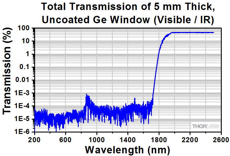
Uncoated Ge Window
Click to Enlarge
Click for Raw Data
This graph shows the full scale measured transmission of an uncoated germanium window at normal incidence.
Click to Enlarge
Click for Raw Data
This graph shows the measured transmission of an uncoated germanium window at normal incidence in the visible wavelength range. The values reported in the visible and near infrared are limited by the noise floor of the spectrometer used. Please note that out-of-band transmission is not monitored during production and will vary from lot to lot.
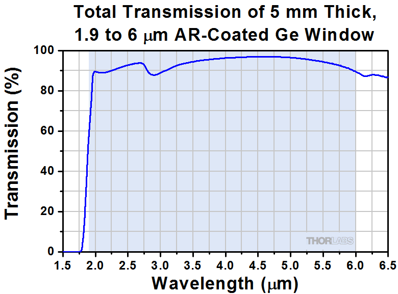
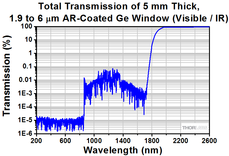
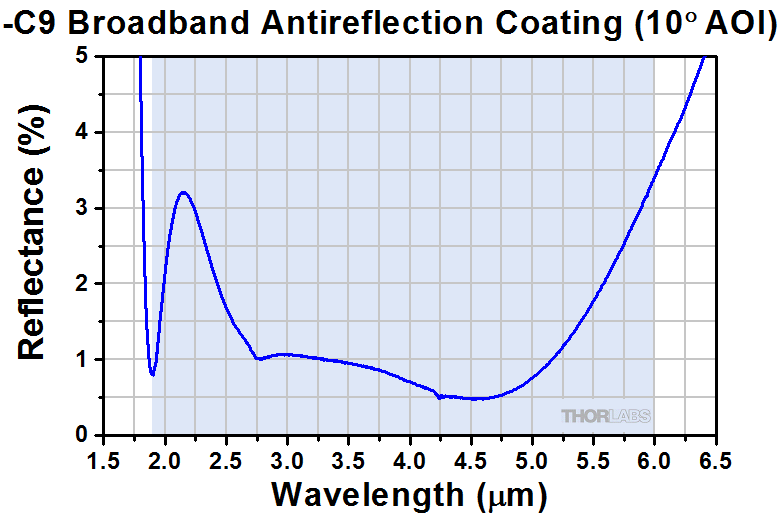
Ge Window, AR Coated for 1.9 to 6 µm
Click to Enlarge
Click for Raw Data
This graph shows the full scale measured transmission of an AR-coated germanium window at normal incidence. The shaded region denotes the AR coating range, over which Ravg < 2% per surface.
Click to Enlarge
Click for Raw Data
This graph shows the measured transmission of a 1.9 to 6 µm AR-coated germanium window at normal incidence in the visible wavelength range. The values reported in the visible and near infrared are limited by the noise floor of the spectrometer used. Please note that out-of-band transmission is not monitored during production and will vary from lot to lot.
Click to Enlarge
Click for Raw Data
This plot gives the measured reflectance (per surface) at normal incidence of our 5 mm thick, AR-coated germanium window. The average reflectance is <2.0% per surface within the shaded wavelength range of 1.9 - 6 µm.
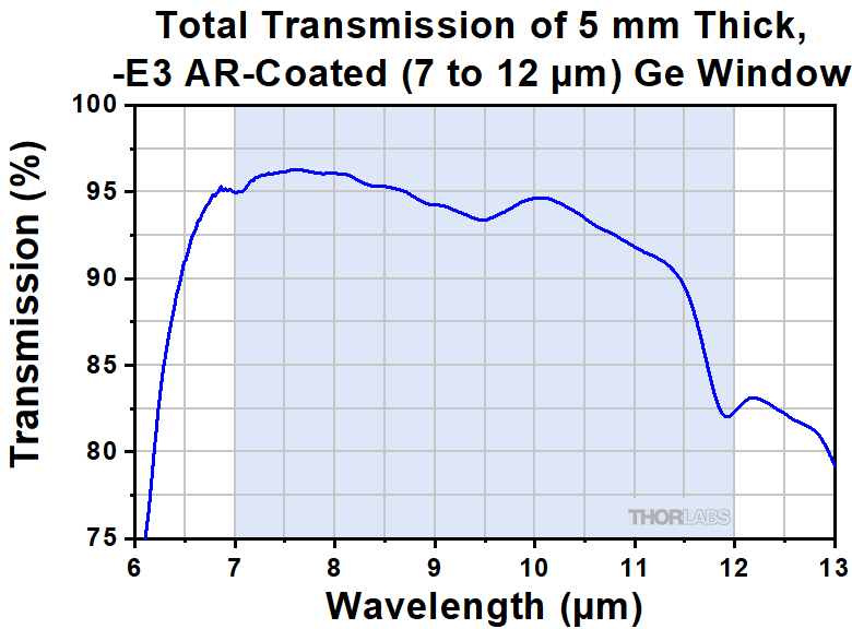
Ge Window, AR Coated for 7 to 12 µm

Click to Enlarge
Click for Raw Data
This plot gives the measured reflectance at of our AR-coated Germanium window. The average reflectance is <1.0% per surface within the shaded wavelength ragne of 7 µm - 12 µm.
Click to Enlarge
Click for Raw Data
Shown above is a graph of the measured transmission of a 5 mm thick -E3 anti-reflection coated germanium substrate. The blue shaded region denotes the 7 µm - 12 µm range of the specified coating.
| Damage Threshold Specifications | |
|---|---|
| Item # | Damage Threshold |
| WG91050-C9 | 10 J/cm2 (2940 nm, 200 µs, 2 Hz, Ø0.485 mm) |
| WG91050-E3 | 0.5 J/cm2 (10.6 µm, 100 ns, 1 Hz, Ø0.478 mm) |
Damage Threshold Data for Thorlabs' Germanium Windows
The specifications to the right are measured data for Thorlabs' germanium windows. Damage threshold specifications are constant for germanium windows with the same coating, regardless of the size of the window.
Laser Induced Damage Threshold Tutorial
The following is a general overview of how laser induced damage thresholds are measured and how the values may be utilized in determining the appropriateness of an optic for a given application. When choosing optics, it is important to understand the Laser Induced Damage Threshold (LIDT) of the optics being used. The LIDT for an optic greatly depends on the type of laser you are using. Continuous wave (CW) lasers typically cause damage from thermal effects (absorption either in the coating or in the substrate). Pulsed lasers, on the other hand, often strip electrons from the lattice structure of an optic before causing thermal damage. Note that the guideline presented here assumes room temperature operation and optics in new condition (i.e., within scratch-dig spec, surface free of contamination, etc.). Because dust or other particles on the surface of an optic can cause damage at lower thresholds, we recommend keeping surfaces clean and free of debris. For more information on cleaning optics, please see our Optics Cleaning tutorial.
Testing Method
Thorlabs' LIDT testing is done in compliance with ISO/DIS 11254 and ISO 21254 specifications.
First, a low-power/energy beam is directed to the optic under test. The optic is exposed in 10 locations to this laser beam for 30 seconds (CW) or for a number of pulses (pulse repetition frequency specified). After exposure, the optic is examined by a microscope (~100X magnification) for any visible damage. The number of locations that are damaged at a particular power/energy level is recorded. Next, the power/energy is either increased or decreased and the optic is exposed at 10 new locations. This process is repeated until damage is observed. The damage threshold is then assigned to be the highest power/energy that the optic can withstand without causing damage. A histogram such as that below represents the testing of one BB1-E02 mirror.
The photograph above is a protected aluminum-coated mirror after LIDT testing. In this particular test, it handled 0.43 J/cm2 (1064 nm, 10 ns pulse, 10 Hz, Ø1.000 mm) before damage.
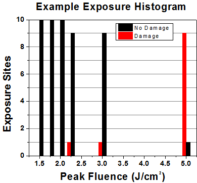
| Example Test Data | |||
|---|---|---|---|
| Fluence | # of Tested Locations | Locations with Damage | Locations Without Damage |
| 1.50 J/cm2 | 10 | 0 | 10 |
| 1.75 J/cm2 | 10 | 0 | 10 |
| 2.00 J/cm2 | 10 | 0 | 10 |
| 2.25 J/cm2 | 10 | 1 | 9 |
| 3.00 J/cm2 | 10 | 1 | 9 |
| 5.00 J/cm2 | 10 | 9 | 1 |
According to the test, the damage threshold of the mirror was 2.00 J/cm2 (532 nm, 10 ns pulse, 10 Hz, Ø0.803 mm). Please keep in mind that these tests are performed on clean optics, as dirt and contamination can significantly lower the damage threshold of a component. While the test results are only representative of one coating run, Thorlabs specifies damage threshold values that account for coating variances.
Continuous Wave and Long-Pulse Lasers
When an optic is damaged by a continuous wave (CW) laser, it is usually due to the melting of the surface as a result of absorbing the laser's energy or damage to the optical coating (antireflection) [1]. Pulsed lasers with pulse lengths longer than 1 µs can be treated as CW lasers for LIDT discussions.
When pulse lengths are between 1 ns and 1 µs, laser-induced damage can occur either because of absorption or a dielectric breakdown (therefore, a user must check both CW and pulsed LIDT). Absorption is either due to an intrinsic property of the optic or due to surface irregularities; thus LIDT values are only valid for optics meeting or exceeding the surface quality specifications given by a manufacturer. While many optics can handle high power CW lasers, cemented (e.g., achromatic doublets) or highly absorptive (e.g., ND filters) optics tend to have lower CW damage thresholds. These lower thresholds are due to absorption or scattering in the cement or metal coating.
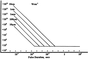
LIDT in linear power density vs. pulse length and spot size. For long pulses to CW, linear power density becomes a constant with spot size. This graph was obtained from [1].
Pulsed lasers with high pulse repetition frequencies (PRF) may behave similarly to CW beams. Unfortunately, this is highly dependent on factors such as absorption and thermal diffusivity, so there is no reliable method for determining when a high PRF laser will damage an optic due to thermal effects. For beams with a high PRF both the average and peak powers must be compared to the equivalent CW power. Additionally, for highly transparent materials, there is little to no drop in the LIDT with increasing PRF.
In order to use the specified CW damage threshold of an optic, it is necessary to know the following:
- Wavelength of your laser
- Beam diameter of your beam (1/e2)
- Approximate intensity profile of your beam (e.g., Gaussian)
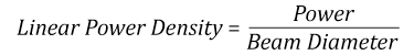
- Linear power density of your beam (total power divided by 1/e2 beam diameter)
Thorlabs expresses LIDT for CW lasers as a linear power density measured in W/cm. In this regime, the LIDT given as a linear power density can be applied to any beam diameter; one does not need to compute an adjusted LIDT to adjust for changes in spot size, as demonstrated by the graph to the right. Average linear power density can be calculated using the equation below.
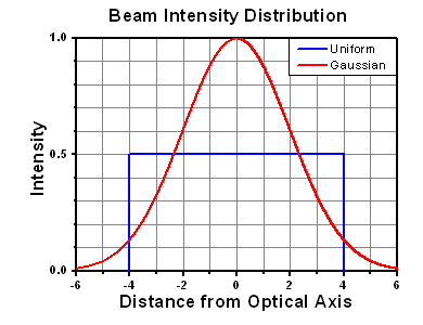
The calculation above assumes a uniform beam intensity profile. You must now consider hotspots in the beam or other non-uniform intensity profiles and roughly calculate a maximum power density. For reference, a Gaussian beam typically has a maximum power density that is twice that of the uniform beam (see lower right).
Now compare the maximum power density to that which is specified as the LIDT for the optic. If the optic was tested at a wavelength other than your operating wavelength, the damage threshold must be scaled appropriately. A good rule of thumb is that the damage threshold has a linear relationship with wavelength such that as you move to shorter wavelengths, the damage threshold decreases (i.e., a LIDT of 10 W/cm at 1310 nm scales to 5 W/cm at 655 nm):
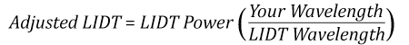
While this rule of thumb provides a general trend, it is not a quantitative analysis of LIDT vs wavelength. In CW applications, for instance, damage scales more strongly with absorption in the coating and substrate, which does not necessarily scale well with wavelength. While the above procedure provides a good rule of thumb for LIDT values, please contact Tech Support if your wavelength is different from the specified LIDT wavelength. If your power density is less than the adjusted LIDT of the optic, then the optic should work for your application.
Please note that we have a buffer built in between the specified damage thresholds online and the tests which we have done, which accommodates variation between batches. Upon request, we can provide individual test information and a testing certificate. The damage analysis will be carried out on a similar optic (customer's optic will not be damaged). Testing may result in additional costs or lead times. Contact Tech Support for more information.
Pulsed Lasers
As previously stated, pulsed lasers typically induce a different type of damage to the optic than CW lasers. Pulsed lasers often do not heat the optic enough to damage it; instead, pulsed lasers produce strong electric fields capable of inducing dielectric breakdown in the material. Unfortunately, it can be very difficult to compare the LIDT specification of an optic to your laser. There are multiple regimes in which a pulsed laser can damage an optic and this is based on the laser's pulse length. The highlighted columns in the table below outline the relevant pulse lengths for our specified LIDT values.
Pulses shorter than 10-9 s cannot be compared to our specified LIDT values with much reliability. In this ultra-short-pulse regime various mechanics, such as multiphoton-avalanche ionization, take over as the predominate damage mechanism [2]. In contrast, pulses between 10-7 s and 10-4 s may cause damage to an optic either because of dielectric breakdown or thermal effects. This means that both CW and pulsed damage thresholds must be compared to the laser beam to determine whether the optic is suitable for your application.
| Pulse Duration | t < 10-9 s | 10-9 < t < 10-7 s | 10-7 < t < 10-4 s | t > 10-4 s |
|---|---|---|---|---|
| Damage Mechanism | Avalanche Ionization | Dielectric Breakdown | Dielectric Breakdown or Thermal | Thermal |
| Relevant Damage Specification | No Comparison (See Above) | Pulsed | Pulsed and CW | CW |
When comparing an LIDT specified for a pulsed laser to your laser, it is essential to know the following:
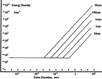
LIDT in energy density vs. pulse length and spot size. For short pulses, energy density becomes a constant with spot size. This graph was obtained from [1].
- Wavelength of your laser
- Energy density of your beam (total energy divided by 1/e2 area)
- Pulse length of your laser
- Pulse repetition frequency (prf) of your laser
- Beam diameter of your laser (1/e2 )
- Approximate intensity profile of your beam (e.g., Gaussian)
The energy density of your beam should be calculated in terms of J/cm2. The graph to the right shows why expressing the LIDT as an energy density provides the best metric for short pulse sources. In this regime, the LIDT given as an energy density can be applied to any beam diameter; one does not need to compute an adjusted LIDT to adjust for changes in spot size. This calculation assumes a uniform beam intensity profile. You must now adjust this energy density to account for hotspots or other nonuniform intensity profiles and roughly calculate a maximum energy density. For reference a Gaussian beam typically has a maximum energy density that is twice that of the 1/e2 beam.
Now compare the maximum energy density to that which is specified as the LIDT for the optic. If the optic was tested at a wavelength other than your operating wavelength, the damage threshold must be scaled appropriately [3]. A good rule of thumb is that the damage threshold has an inverse square root relationship with wavelength such that as you move to shorter wavelengths, the damage threshold decreases (i.e., a LIDT of 1 J/cm2 at 1064 nm scales to 0.7 J/cm2 at 532 nm):
You now have a wavelength-adjusted energy density, which you will use in the following step.
Beam diameter is also important to know when comparing damage thresholds. While the LIDT, when expressed in units of J/cm², scales independently of spot size; large beam sizes are more likely to illuminate a larger number of defects which can lead to greater variances in the LIDT [4]. For data presented here, a <1 mm beam size was used to measure the LIDT. For beams sizes greater than 5 mm, the LIDT (J/cm2) will not scale independently of beam diameter due to the larger size beam exposing more defects.
The pulse length must now be compensated for. The longer the pulse duration, the more energy the optic can handle. For pulse widths between 1 - 100 ns, an approximation is as follows:
Use this formula to calculate the Adjusted LIDT for an optic based on your pulse length. If your maximum energy density is less than this adjusted LIDT maximum energy density, then the optic should be suitable for your application. Keep in mind that this calculation is only used for pulses between 10-9 s and 10-7 s. For pulses between 10-7 s and 10-4 s, the CW LIDT must also be checked before deeming the optic appropriate for your application.
Please note that we have a buffer built in between the specified damage thresholds online and the tests which we have done, which accommodates variation between batches. Upon request, we can provide individual test information and a testing certificate. Contact Tech Support for more information.
[1] R. M. Wood, Optics and Laser Tech. 29, 517 (1998).
[2] Roger M. Wood, Laser-Induced Damage of Optical Materials (Institute of Physics Publishing, Philadelphia, PA, 2003).
[3] C. W. Carr et al., Phys. Rev. Lett. 91, 127402 (2003).
[4] N. Bloembergen, Appl. Opt. 12, 661 (1973).

In order to illustrate the process of determining whether a given laser system will damage an optic, a number of example calculations of laser induced damage threshold are given below. For assistance with performing similar calculations, we provide a spreadsheet calculator that can be downloaded by clicking the button to the right. To use the calculator, enter the specified LIDT value of the optic under consideration and the relevant parameters of your laser system in the green boxes. The spreadsheet will then calculate a linear power density for CW and pulsed systems, as well as an energy density value for pulsed systems. These values are used to calculate adjusted, scaled LIDT values for the optics based on accepted scaling laws. This calculator assumes a Gaussian beam profile, so a correction factor must be introduced for other beam shapes (uniform, etc.). The LIDT scaling laws are determined from empirical relationships; their accuracy is not guaranteed. Remember that absorption by optics or coatings can significantly reduce LIDT in some spectral regions. These LIDT values are not valid for ultrashort pulses less than one nanosecond in duration.
A Gaussian beam profile has about twice the maximum intensity of a uniform beam profile.
CW Laser Example
Suppose that a CW laser system at 1319 nm produces a 0.5 W Gaussian beam that has a 1/e2 diameter of 10 mm. A naive calculation of the average linear power density of this beam would yield a value of 0.5 W/cm, given by the total power divided by the beam diameter:
However, the maximum power density of a Gaussian beam is about twice the maximum power density of a uniform beam, as shown in the graph to the right. Therefore, a more accurate determination of the maximum linear power density of the system is 1 W/cm.
An AC127-030-C achromatic doublet lens has a specified CW LIDT of 350 W/cm, as tested at 1550 nm. CW damage threshold values typically scale directly with the wavelength of the laser source, so this yields an adjusted LIDT value:
The adjusted LIDT value of 350 W/cm x (1319 nm / 1550 nm) = 298 W/cm is significantly higher than the calculated maximum linear power density of the laser system, so it would be safe to use this doublet lens for this application.
Pulsed Nanosecond Laser Example: Scaling for Different Pulse Durations
Suppose that a pulsed Nd:YAG laser system is frequency tripled to produce a 10 Hz output, consisting of 2 ns output pulses at 355 nm, each with 1 J of energy, in a Gaussian beam with a 1.9 cm beam diameter (1/e2). The average energy density of each pulse is found by dividing the pulse energy by the beam area:
As described above, the maximum energy density of a Gaussian beam is about twice the average energy density. So, the maximum energy density of this beam is ~0.7 J/cm2.
The energy density of the beam can be compared to the LIDT values of 1 J/cm2 and 3.5 J/cm2 for a BB1-E01 broadband dielectric mirror and an NB1-K08 Nd:YAG laser line mirror, respectively. Both of these LIDT values, while measured at 355 nm, were determined with a 10 ns pulsed laser at 10 Hz. Therefore, an adjustment must be applied for the shorter pulse duration of the system under consideration. As described on the previous tab, LIDT values in the nanosecond pulse regime scale with the square root of the laser pulse duration:
This adjustment factor results in LIDT values of 0.45 J/cm2 for the BB1-E01 broadband mirror and 1.6 J/cm2 for the Nd:YAG laser line mirror, which are to be compared with the 0.7 J/cm2 maximum energy density of the beam. While the broadband mirror would likely be damaged by the laser, the more specialized laser line mirror is appropriate for use with this system.
Pulsed Nanosecond Laser Example: Scaling for Different Wavelengths
Suppose that a pulsed laser system emits 10 ns pulses at 2.5 Hz, each with 100 mJ of energy at 1064 nm in a 16 mm diameter beam (1/e2) that must be attenuated with a neutral density filter. For a Gaussian output, these specifications result in a maximum energy density of 0.1 J/cm2. The damage threshold of an NDUV10A Ø25 mm, OD 1.0, reflective neutral density filter is 0.05 J/cm2 for 10 ns pulses at 355 nm, while the damage threshold of the similar NE10A absorptive filter is 10 J/cm2 for 10 ns pulses at 532 nm. As described on the previous tab, the LIDT value of an optic scales with the square root of the wavelength in the nanosecond pulse regime:
This scaling gives adjusted LIDT values of 0.08 J/cm2 for the reflective filter and 14 J/cm2 for the absorptive filter. In this case, the absorptive filter is the best choice in order to avoid optical damage.
Pulsed Microsecond Laser Example
Consider a laser system that produces 1 µs pulses, each containing 150 µJ of energy at a repetition rate of 50 kHz, resulting in a relatively high duty cycle of 5%. This system falls somewhere between the regimes of CW and pulsed laser induced damage, and could potentially damage an optic by mechanisms associated with either regime. As a result, both CW and pulsed LIDT values must be compared to the properties of the laser system to ensure safe operation.
If this relatively long-pulse laser emits a Gaussian 12.7 mm diameter beam (1/e2) at 980 nm, then the resulting output has a linear power density of 5.9 W/cm and an energy density of 1.2 x 10⁻⁴ J/cm2 per pulse. This can be compared to the LIDT values for a WPQ10E-980 polymer zero-order quarter-wave plate, which are 5 W/cm for CW radiation at 810 nm and 5 J/cm2 for a 10 ns pulse at 810 nm. As before, the CW LIDT of the optic scales linearly with the laser wavelength, resulting in an adjusted CW value of 6 W/cm at 980 nm. On the other hand, the pulsed LIDT scales with the square root of the laser wavelength and the square root of the pulse duration, resulting in an adjusted value of 55 J/cm2 for a 1 µs pulse at 980 nm. The pulsed LIDT of the optic is significantly greater than the energy density of the laser pulse, so individual pulses will not damage the wave plate. However, the large average linear power density of the laser system may cause thermal damage to the optic, much like a high-power CW beam.
| Posted Comments: | |
user
(posted 2022-06-09 02:35:45.373) Can the uncoated Germanium glass be used at -40 deg C? Or is there any max negative temperature for Ge?
Thank You! cdolbashian
(posted 2022-06-21 09:43:24.0) Thank you for reaching out with this inquiry. After further discussion, we concluded that you are interested in the transmission data for this material at -40C. We unfortunately do not have this data as we have not tested our germanium windows in this manner. I have contacted you directly with some supplementary information I found on the web. Charles Drutman
(posted 2021-09-09 10:01:14.317) For germanium windows, is the sample defect-free or are there nano-particles of foreign materials? I need to know this in order to model damage, as nano-particles have different thermal profiles than the host material, and this is expressed in the damage process. Many thanks. azandani
(posted 2021-09-16 11:05:50.0) Hello Charles, thank you for contacting Thorlabs. The material is >99.999% purity Germanium, but we can not test for or guarantee that there are no foreign materials in a lower concentration than this. I will reach out to you directly to provide documentation regarding this. user
(posted 2013-03-14 08:37:05.127) It would be great if you could provide much broader transmission plots. Often need to know the transmission in the visible so we can sneak in an alignment laser. sharrell
(posted 2013-03-14 10:18:00.0) Response from Sean at Thorlabs: Thank you for your feedback! We have added extended transmission plots down to 200 nm. Unfortunately, Ge does not transmit visible light. We also offer ZnSe windows, which do offer good transmsission in the infrared and visible regions (http://www.thorlabs.com/newgrouppage9.cfm?objectgroup_id=3981). We will continue adding visible transmission plots to our infrared optics in the coming months. tcohen
(posted 2012-10-15 09:32:00.0) Response from Tim at Thorlabs: Two possible options will be Ge and ZnSe. We will generate some data on performance with the –F coatings and contact you directly to discuss your requirements. dylan.martin
(posted 2012-10-11 12:37:30.853) Am looking for an IR window to effectively use as a beam splitter between LWIR and NIR bands. Ultimately, looking for a window/beamsplitter that can transmit LWIR 8-12um for one arm, and reflect NIR 1um for second arm. What window would be ideal for this application? tcohen
(posted 2012-10-04 15:43:00.0) Response from Tim at Thorlabs: Ge becomes increasingly more absorptive in the lower end of your spectrum and will limit transmission. I will contact you to provide updates as we accumulate data within this wavelength region with the -F ARC. nick
(posted 2012-10-04 11:27:51.0) Hello- Can you tell me what the R/T performance is from 1-2um (at least on an example run, if not well-controlled) at both 0 and 45 degree AOI? tcohen
(posted 2012-03-22 10:06:00.0) Response from Tim at Thorlabs: Thank you for your feedback. The resistivity range of the Germanium we utilize is 5-40 Ohm-cm. Also, we are able to offer custom coatings on some of our optics. I have contacted you directly to get more information. nick
(posted 2012-03-20 10:36:24.0) Can you please inform me if you can provide these Ge windows with diamond-like coating (DLC) on a single surface (and then uncoated or AR on the other)? Also, what is the allowed resistivity range of the Ge you utilize (in ohm-cm)? bdada
(posted 2011-09-22 20:34:00.0) Response from Buki at Thorlabs:
Thank you for using our Feedback tool. Yes, you can use these Germanium windows at a 45 degree angle to function as a beam sampler. tttang
(posted 2011-09-13 22:23:00.0) Could we use this Ge window as a beamsplitter for 45 deg incident with a small mount reflection? We would like to find a BS for pump-probe system for around 8um. Thank you. jjurado
(posted 2011-08-29 10:25:00.0) Response from Javier at Thorlabs to mhlavach: We currently do not have information regarding the performance of our Ge windows in the 1000 to 1200 °C range. The coating process used goes up to about 100 °C, but we do not have any data at higher temperatures. mhlavach
(posted 2011-08-26 16:34:18.0) Can germanium windows survive a combustion environment of 1000 to 1200C? nick
(posted 2010-11-09 13:17:12.0) Can you please report the surface reflection around 1um wavelength? |
| Window Selection Guide (Table Sorted by Wavelength) | |||||
|---|---|---|---|---|---|
| Substrate and Window Type | Wavelength Range | Available AR Coatings | Reflectance over AR Coating Rangea | Transmission Data | Reflectance Data |
| Calcium Fluoride (CaF2): Flat or Wedged |
180 nm - 8.0 μm | Uncoated | - | Raw Data |
- |
| -D Coating, 1.65 - 3.0 µm | Ravg < 1.0%; Rabs < 2.0% at 0° AOI | Raw Data |
Raw Data |
||
| UV Fused Silica: Flat, Wedged, V-Coated Flat, or V-Coated Wedged |
185 nm - 2.1 μm | Uncoated (Flat or Wedged) |
- | Raw Data |
- |
| -UV Coating, 245 - 400 nm (Flat or Wedged) |
Ravg < 0.5% at 0° AOI | - | Raw Data |
||
| -C3 Coating, 261 - 266 nm (V-Coated) |
Ravg < 0.5% at 0° AOI | - | Raw Data |
||
| -C6 Coating, 350 - 450 nm (V-Coated) |
Ravg < 0.5% at 0° AOI | - | Raw Data |
||
| -A Coating, 350 - 700 nm (Flat or Wedged) |
Ravg < 0.5% at 0° AOI | - | Raw Data |
||
| -B Coating, 650 - 1050 nm (Flat or Wedged) |
Ravg < 0.5% at 0° AOI | - | Raw Data |
||
| -C Coating, 1050 - 1700 nm (Flat or Wedged) |
Ravg < 0.5% at 0° AOI | - | Raw Data |
||
| Sapphire: Flat or Wedged |
200 nm - 5.0 μm | Uncoated | - | Raw Data |
- |
| -D Coating, 1.65 - 3.0 µm | Ravg < 1.0% at 0° AOI | Raw Data |
Raw Data |
||
| -E1 Coating, 2.0 - 5.0 µm | Ravg < 1.50%, Rabs < 3.0% (per Surface, 2.0 - 5.0 µm); Ravg < 1.75% (per Surface, 2.0 - 4.0 µm) at 0° AOI |
Raw Data |
Raw Data |
||
| Magnesium Fluoride (MgF2): Flat or Wedged |
200 nm - 6.0 μm | Uncoated | - | Raw Data |
- |
| Barium Fluoride (BaF2): Flat or Wedged |
200 nm - 11 µm | Uncoated (Wedged Only) |
- |  Raw Data |
- |
| -E1 Coating, 2 - 5 µm | Ravg < 1.25%; Rabs < 2.5% at 0° AOI | Raw Data |
Raw Data |
||
| UV Fused Silica, for 45° AOI: Flat or Wedged |
250 nm - 1.6 µm | Coating for 250 nm - 450 nm |
Ravg < 1.0% at 45° AOI | Raw Data |
|
| Coating for 350 nm - 1100 nm |
Ravg < 2.0% at 45° AOI | Raw Data |
|||
| Coating for 400 nm - 700 nm |
Ravg < 1.0% at 45° AOI | Raw Data |
|||
| Coating for 600 nm - 1700 nm |
Ravg < 1.5% at 45° AOI | Raw Data |
|||
| Coating for 700 nm - 1100 nm |
Ravg < 1.0% at 45° AOI | Raw Data |
|||
| Coating for 1200 nm - 1600 nm |
Ravg < 1.0% at 45° AOI | Raw Data |
|||
| Potassium Bromide (KBr): Flat |
250 nm - 26 µm | Uncoated | - | - | |
| Infrasil®: Flat |
300 nm - 3 µm | Uncoated | - | Raw Data |
- |
| N-BK7: Flat, Wedged, V-Coated Flat, or V-Coated Wedged |
350 nm - 2.0 μm | Uncoated (Flat or Wedged) |
- | Raw Data |
- |
| -A Coating, 350 - 700 nm (Flat or Wedged) |
Ravg < 0.5% at 0° AOI | - | Raw Data |
||
| -C7 Coating, 400 - 700 nm (V-Coated) |
Ravg < 0.5% at 0° AOI | - | Raw Data |
||
| -C10 Coating, 523 - 532 nm (V-Coated) |
Ravg < 0.5% at 0° AOI | - | Raw Data |
||
| -C11 Coating, 610 - 860 nm (V-Coated) |
Ravg < 0.5% at 0° AOI | - | Raw Data |
||
| -B Coating, 650 - 1050 nm (Flat or Wedged) |
Ravg < 0.5% at 0° AOI | - | Raw Data |
||
| -C13 Coating, 700 - 1100 nm (V-Coated) |
Ravg < 0.5% at 0° AOI | - | Raw Data |
||
| C14 Coating, 1047 - 1064 nm (V-Coated) |
Ravg < 0.5% at 0° AOI | - | Raw Data |
||
| -C15 Coating, 523 - 532 nm & 1047 - 1064 nm (V-Coated) |
Ravg < 0.5% at 0° AOI | - | Raw Data |
||
| -C Coating, 1050 - 1700 nm (Flat or Wedged) |
Ravg < 0.5% at 0° AOI | - | Raw Data |
||
| Zinc Selenide (ZnSe): Flat or Wedged |
600 nm - 16 µm | Uncoated | - | Raw Data |
- |
| -D Coating, 1.65 - 3.0 µm | Ravg < 1.0%; Rabs < 2.0% at 0° AOI | Raw Data |
Raw Data |
||
| -E4 Coating, 2 - 13 µm (Only Flat) |
Ravg < 3.5%; Rabs < 6% at 0° AOI | Raw Data |
Raw Data |
||
| -E2 Coating, 4.5 - 7.5 µm (Only Flat) |
Ravg < 1.0%; Rabs < 2.0% at 0° AOI | Raw Data |
Raw Data |
||
| -E3 Coating, 7 - 12 µm (Only Wedged) |
Ravg < 1.0%; Rabs < 2.0% at 0° AOI | Raw Data |
Raw Data |
||
| -G Coating, 7 - 12 µm (Only Flat) |
Ravg < 1% at 0° AOI | Raw Data |
Raw Data |
||
| Silicon (Si): Flat or Wedged |
1.2 - 8.0 μm | Uncoated | - | Raw Data |
- |
| -E1 Coating, 2 - 5 µm (Only Wedged) |
Ravg < 1.25%; Rabs < 2.5% at 0° AOI | Raw Data |
Raw Data |
||
| -E Coating, 3 - 5 µm (Only Flat) |
Ravg < 2% at 0° AOI | Raw Data |
Raw Data |
||
| Germanium (Ge): Flat or Wedged |
1.9 - 16 μm | Uncoated, 2.0 - 16 μm | - | Raw Data |
- |
| -C9 Coating, 1.9 - 6 µm (Only Flat) |
Ravg < 2% at 0° AOI | Raw Data |
Raw Data |
||
| -E3 Coating, 7 - 12 µm | Ravg < 1.0%; Rabs < 2.0% at 0° AOI | Raw Data |
Raw Data |
||

 Zoom
Zoom| Item # | WG90530 | WG91050 |
|---|---|---|
| Diameter | 1/2" (12.7 mm) | 1" (25.4 mm) |
| Diameter Tolerance | +0.0 / -0.2 mm | |
| Thickness | 3.0 mm | 5.0 mm |
| Thickness Tolerance | ±0.1 mm | |
| Clear Aperture | ≥Ø11.43 mm | ≥Ø22.86 mm |
| Parallelism | ≤1 arcmin | <1 arcmin |
| Surface Flatnessa | ≤λ over Clear Aperture | |
| Surface Quality | 40-20 Scratch-Dig | |
| Wavelength Range | 2.0 - 16 μm (Uncoated) | |
| Substrate | Germaniumb | |
| Transmission Data (Click for Graph) |
Raw Data |
|

 Zoom
Zoom| Item # | WG91050-C9 | |
|---|---|---|
| Diameter | 1" (25.4 mm) | |
| Diameter Tolerance | +0.0 / -0.2 mm | |
| Thickness | 5.0 mm | |
| Thickness Tolerance | ±0.1 mm | |
| Clear Aperture | ≥Ø22.86 mm | |
| Parallelism | <1 arcmin | |
| Surface Flatnessa | <λ over Clear Aperture | |
| Surface Quality | 40-20 Scratch-Dig | |
| AR Coating Range | 1.9 - 6 µm (-C9 Coating) | |
| Reflectance over AR Coating Rangeb | Ravg < 2% | |
| Reflectance Data (Click for Graph) |
Raw Data |
|
| Substrate | Germaniumc | |
| Transmission Data (Click for Graph) |
Raw Data |
|
| Damage Threshold | 10 J/cm2 (2940 nm, 200 µs, 2 Hz, Ø0.485 mm) | |

 Zoom
Zoom| Item # | WG90530-E3 | WG91050-E3 | |
|---|---|---|---|
| Diameter | 1/2" (12.7 mm) | 1" (25.4 mm) | |
| Diameter Tolerance | +0.0 / -0.2 mm | ||
| Thickness | 3.0 mm | 5.0 mm | |
| Thickness Tolerance | ±0.1 mm | ||
| Clear Aperture | ≥Ø11.4 mm | ≥Ø22.9 mm | |
| Parallelism | ≤1 arcmin | ||
| Surface Flatnessa | ≤λ over Clear Aperture | ||
| Surface Quality | 40-20 Scratch-Dig | ||
| AR Coating Range | 7 - 12 µm (-E3 Coating) | ||
| Reflectance over AR Coating Rangeb | Ravg < 1.0%, Rabs < 2.0% | ||
| Transmission over AR Coating Rangec | 7 - 11 µm: Tavg > 94%, Tabs > 90% 11 - 12 µm: Tavg > 85%, Tabs > 80% |
||
| Reflectance Data (Click for Graph) |
 Raw Data |
||
| Substrate | Germaniumd | ||
| Transmission Data (Click for Graph) |
Raw Data |
||
| Damage Threshold | 0.5 J/cm2 (10.6 µm, 100 ns, 1 Hz, Ø0.478 mm) | ||