 Products Home / Custom Solutions & Manufacturing Capabilities / Thorlabs Semiconductor Manufacturing Capabilities
Thorlabs Semiconductor Manufacturing Capabilities

Please Wait
Thorlabs Semiconductor Manufacturing Capabilities
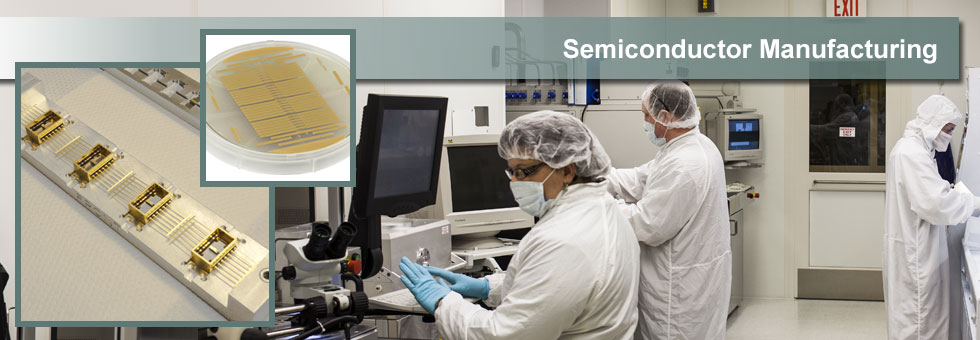
Thorlabs Semiconductor Manufacturing
Thorlabs manufactures a broad variety of active optical devices, including III-V semiconductor devices, MEMS-VCSEL lasers, quantum cascade lasers, and lithium niobate optical modulators. Our vertically integrated semiconductor manufacturing facility in Jessup, Maryland allows us to produce fully packaged custom and OEM products as well as our stock catalog offerings.
Click on the tabs above or the banner below to explore our semiconductor product line and learn about our capabilities for each step of the manufacturing process.

Semiconductor Products Manufactured by Thorlabs
Thorlabs has fabrication and packaging capabilities for group III-V (InP, GaAs, GaSb) semiconductor devices, mid-IR quantum cascade and interband cascade lasers (QCLs and ICLs), and lithium niobate (LiNbO3) electro-optic modulators. These products are manufactured at our Thorlabs Quantum Electronics (TQE) facility in Jessup, Maryland. Our products include the following:
- III-V Optical Semiconductor Devices
- Laser Diodes
- Optical Amplifiers (Semiconductor and Booster Optical Amplifiers)
- Gain Chips
- Superluminescent Diodes
- Single Frequency Lasers (External Cavity, Distributed Feedback, and Distributed Bragg Reflector)
- VCSEL (Vertical Cavity Surface Emitting Lasers)
- Mid-IR Lasers (Quantum Cascade Lasers and Interband Cascade Lasers)
- LiNbO3 Optical Modulators
In addition to our catalog product offerings, which are hyperlinked in the tables below, we have extensive OEM/custom product capabilities. See the OEM/Custom Ordering tab for details.
Components
| III-V Semiconductor Product Line |
|---|
| Fabry-Perot Lasers |
| 785 nm |
| 1260 - 1360 nm (O Band) |
| 1530 - 1565 nm (C Band) |
| 1565 - 1625 nm (L Band) |
| 1625 - 1675 nm (U Band) |
| 1900 - 2000 nm |
| See our TO-Can, Butterfly Package, and Chip on Submount Laser Diodes. |
| Single Frequency Lasers |
| 1550 nm |
| 1620 nm |
| Benchtop DFB Laser Source |
| Optical Amplifiers |
| 1050 nm BOAs |
| 1275 - 1310 nm BOAs (O-Band) |
| 1410 nm BOAs (E-Band) |
| 1550 nm BOAs and SOAs (C-Band) |
| 1590 - 1625 nm BOAs (L-Band) |
| Gain Chips |
| 1220 nm SAF Gain Chips |
| 1320 nm SAF Gain Chips |
| 1450 nm SAF Gain Chips |
| 1550 and 1590 nm SAF Gain Chips |
| 1650 nm SAF Gain Chips |
| Half-Butterfly Gain Chips 770, 1050, 1220, 1320, 1550, and 1900 nm SAF and Fabry Pérot Gain Chips with Thermoelectric Cooler (TEC) |
| Superluminescent Diodes (SLDs) |
| 830 nm - 1550 nm SLDs |
| 830 nm - 1325 nm SLD for Spectral Domain OCT Imaging |
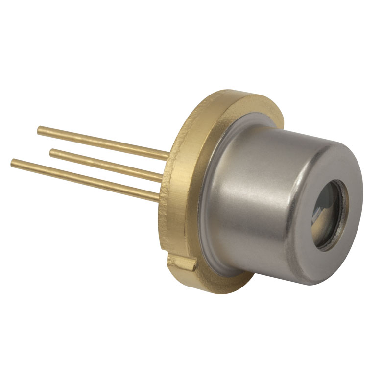
III-V Optical Semiconductor Devices (InP, GaAs, and GaSb)
Our extensive InP, GaAs, and GaSb manufacturing capabilities include solid-source Molecular Beam Epitaxy (MBE) for wafer growth, wafer-level fabrication, optical facet coating, hermetically sealed optoelectronic packaging, and extensive environmental, performance, and reliability testing. We offer an extensive catalog product line, including Fabry-Perot lasers; optical amplifiers including semiconductor optical amplifiers (SOAs) and booster optical amplifiers (BOAs); single angled facet (SAF) and Fabry-Perot gain chips; external cavity (ECL), distributed feedback (DFB), and distributed Bragg reflector (DBR) single-frequency lasers, and superluminescent diodes (SLDs). Our GaSb fabrication capabilities allow for semiconductor optical devices operating in the 2 - 3 µm wavelength range. Custom and OEM devices are also available.
Click to Enlarge
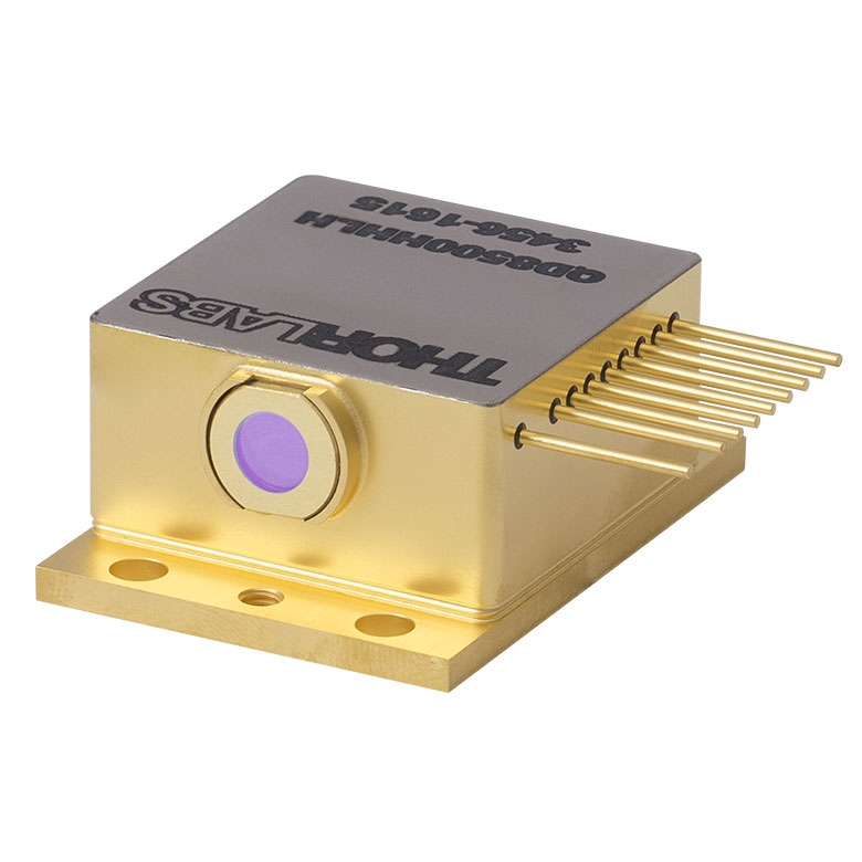
Fabry-Perot Laser Diode

Click to Enlarge
Half-Butterfly Gain Chip
Click to Enlarge
TO Can Laser Diode
MEMS-VCSEL Tunable Lasers
An extension of our III-V product line is our MEMS-VCSEL tunable lasers. Vertical Cavity Surface Emitting Lasers (VCSELs) have the laser cavity orthogonal to the crystal plane. The top cavity mirror is suspended above an air gap by a micro-electro-mechanical system (MEMS), which can move the mirror, changing the cavity length. This design allows for tuning over a wavelength range of approximately 100 nm with rapid sweeping also possible. Compared to edge-emitting sources, VCSELs also offer superior output beam quality and single longitudinal mode operation.
| Mid-IR QCL and ICL Product Line | |
|---|---|
| Fabry-Perot | Two-Tab C-Mount |
| DFB | Two-Tab C-Mount |
| D-Mount | |
| High Heat Load | |
High-Power Fabry-Perot QCLs
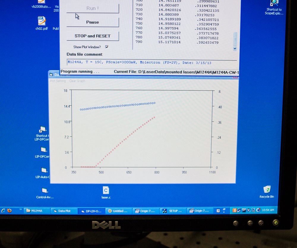
Thorlabs maintains laser chip inventory from 3 µm to 12 µm at our Jessup, Maryland manufacturing facility, and can reach multi-watt output on certain custom orders.
Click to Enlarge
Maximum Output Power of Custom Fabry-Perot QCLs
Mid-IR Lasers
Thorlabs has added manufacturing capabilities for quantum cascade lasers (QCLs) and interband cascade lasers (ICLs) for the mid-IR spectral range (3 - 12 µm). These devices, composed of multiple quantum well heterostructures, utilize intersubband (QCLs) or interband (ICLs) transitions in order to access the mid-infrared spectral region. Our Fabry-Perot QCLs and ICLs have a spectral width of roughly 50 cm-1, while our distributed feedback (DFB) QCLs emit at a single frequency within a tuning range of 1 - 5 cm-1.
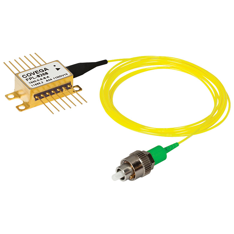
| Fiber-Pigtailed LiNbO3 Modulator Product Line |
|---|
| Intensity, Phase or IQ Modulators |
Lithium Niobate Optical Modulators
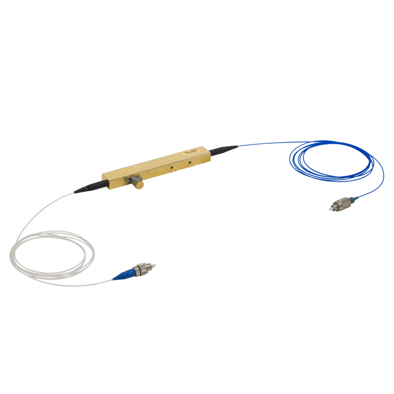
We have extensive lithium niobate (LiNbO3) wafer fabrication and hermetic packaging capabilities, as well as extensive environmental, performance, and reliability testing. Our fiber-coupled intensity and phase modulator products are available with modulation bandwidths of 10 GHz or 40 GHz. They function in the C and L telecommunications bands and are Telcordia GR-468 compliant.
Click to Enlarge
Fiber-Coupled LiNbO3 Optical Modulator
Click to Enlarge
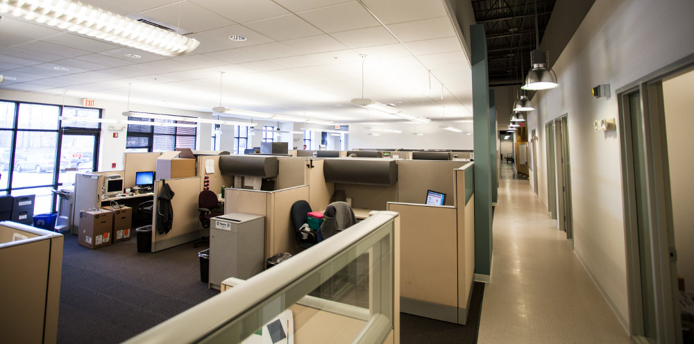
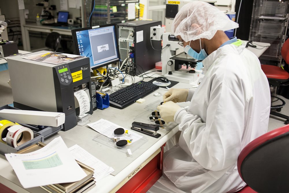
Office and Design Area
Design Capabilities
Our team of engineers utilizes a large selection of tools and design capabilities to support new and existing product development and manufacturing.
- Waveguide Modeling: OptiBPM (Optiwave), BeamPROP (RSoft), and FIMMPROP (Photon Design)
- Laser Simulation: PICS3D (Crosslight) and Proprietary In-House Software
- Extensive Epitaxial Wafer Design, Mechanical Design (Solidworks), Optical Design (Zemax), Thermal Modeling (Comson), and Electrical Design (Altium) Capabilities
Our chip-level design capabilities include optical waveguide design, analysis, and simulation using BeamPROP and FIMMPROP. This gives Thorlabs the ability to study novel waveguide structures. Our laser simulation capabilities include COMSOL Multiphysics as well as proprietary in-house software for epitaxial wafer design. We also have design tools to support opto-mechanical packaging of components including mechanical design using Solidworks, thermal modeling using COSMOS and COMSOL Multiphysics, optical design using Zemax, RF design using Sonnet and electrical design/ layout using Altium. Our engineering design work is supported by extensive optical, electrical and RF test capability for characterization of device performance.
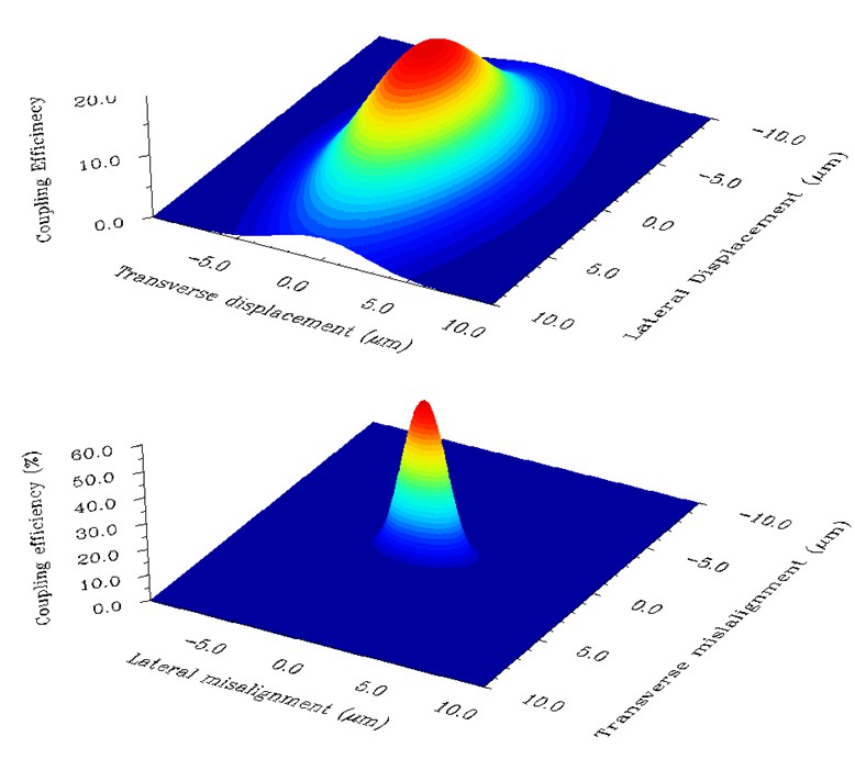
Click to Enlarge
Laser Diode Coupling Efficiency Calculation
Click to Enlarge
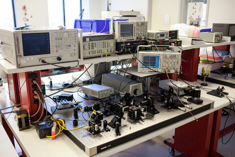
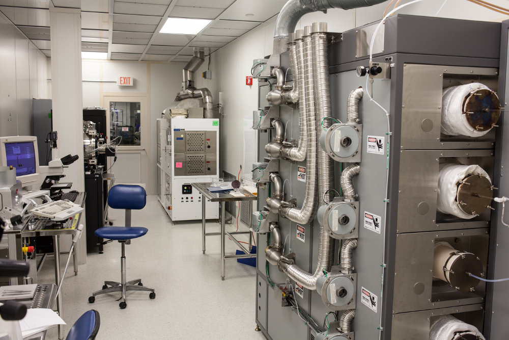
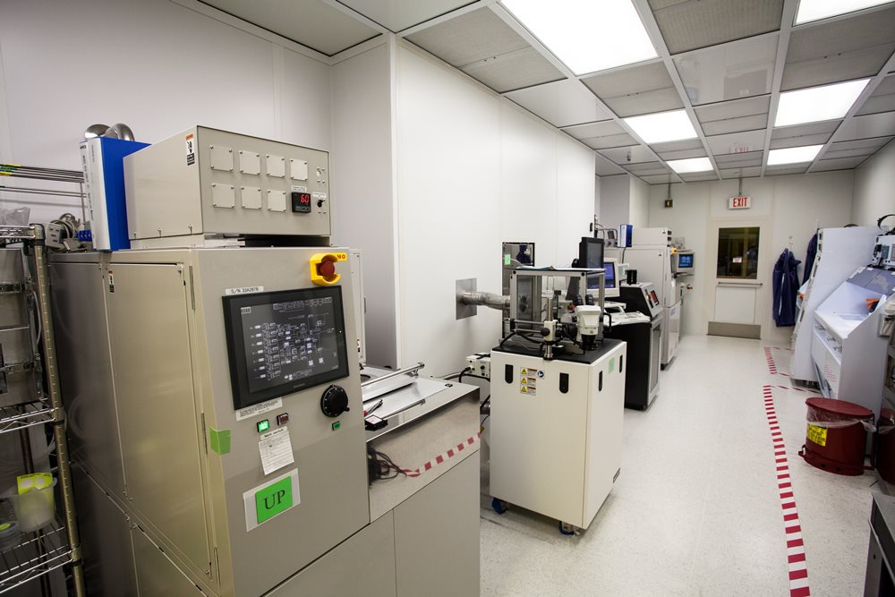
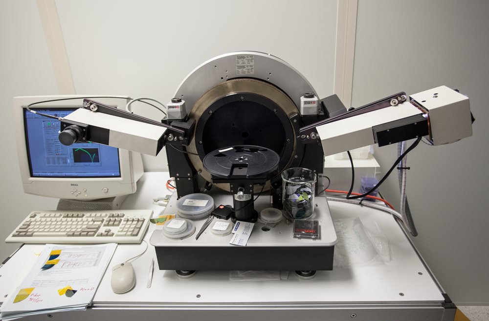
Test Area for Prototyping
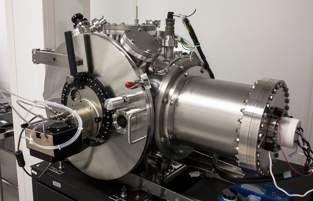
Click to Enlarge
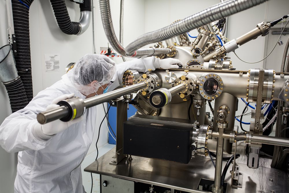
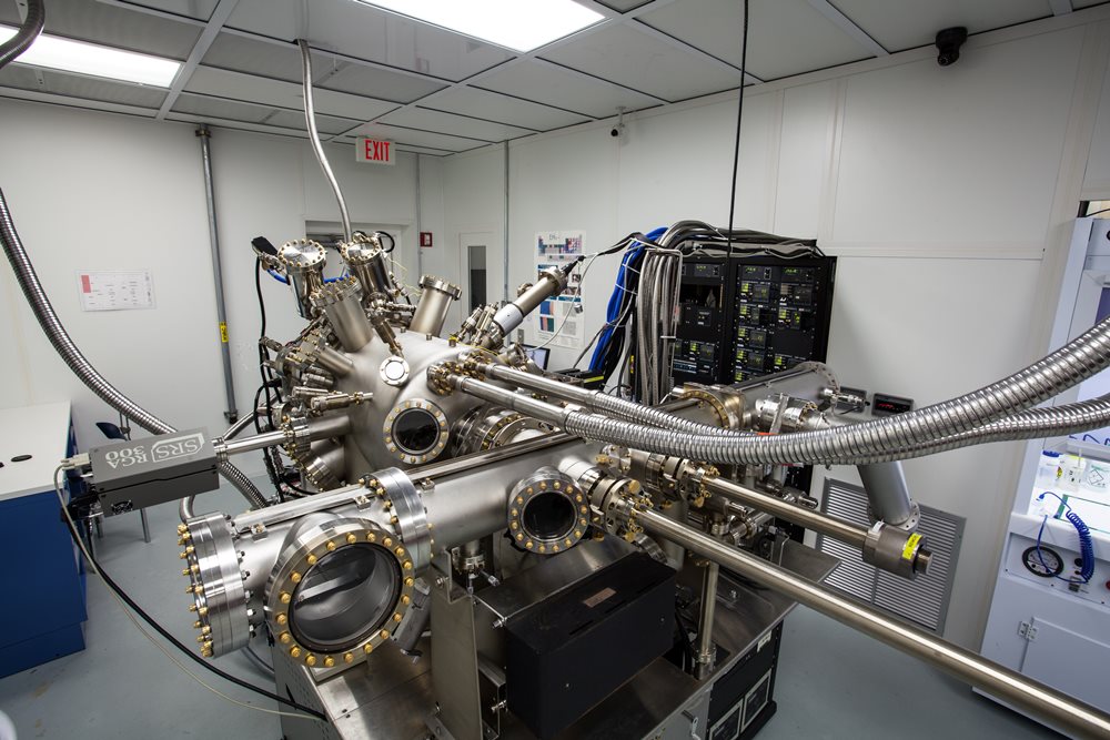
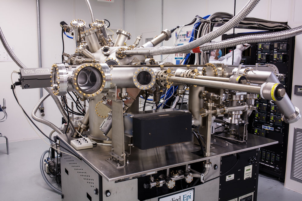
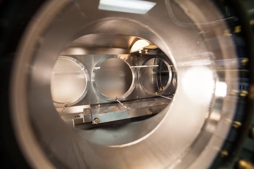
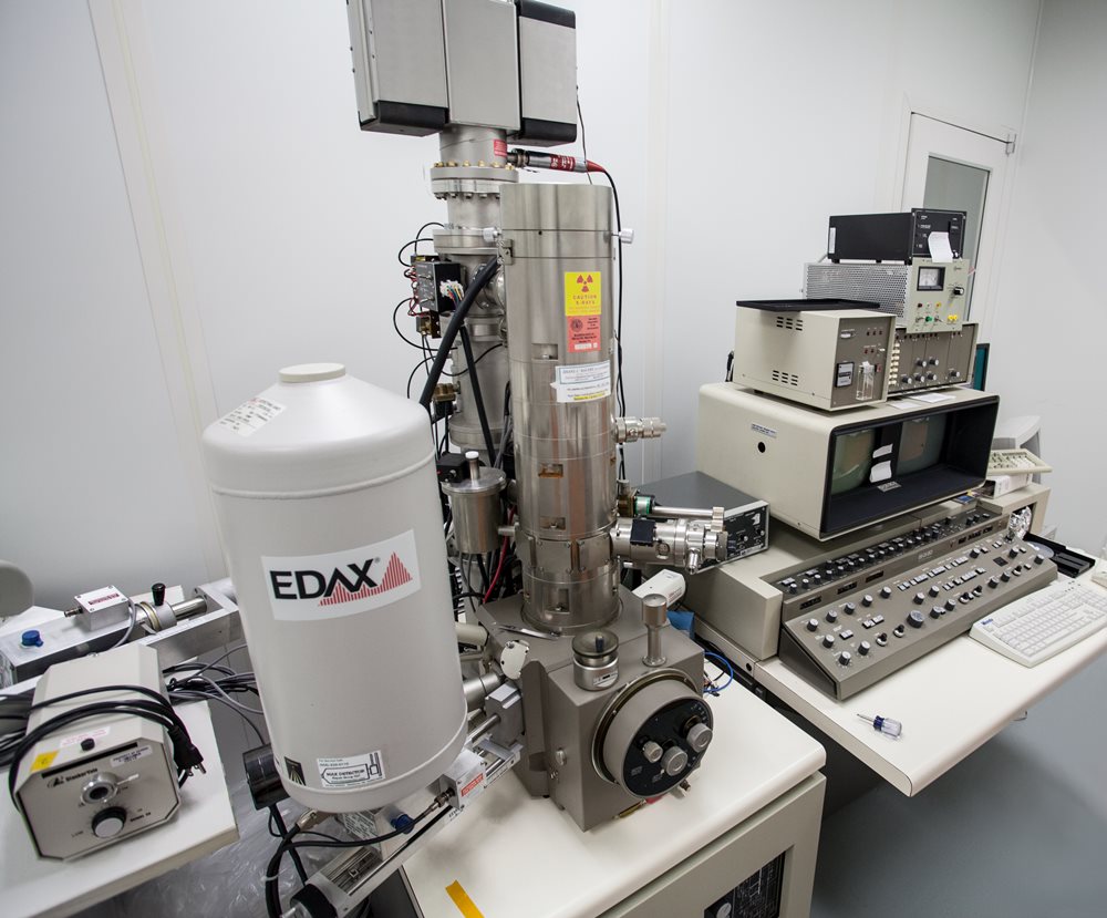
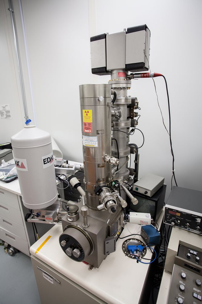
Molecular Beam Epitaxy (MBE) Equipment
Click to Enlarge
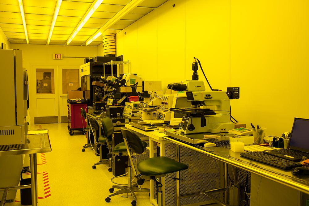
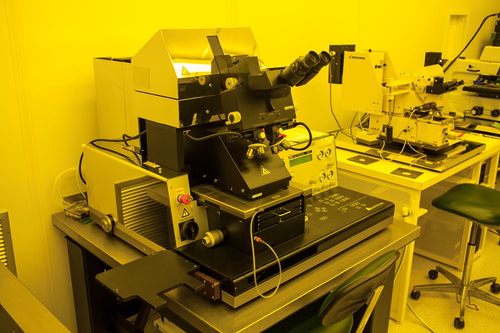
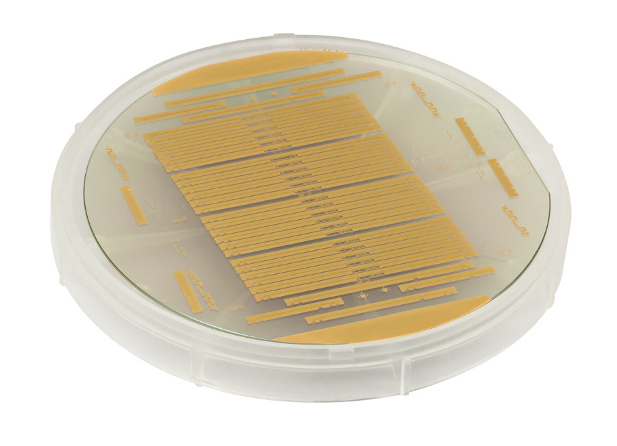
Class 100 Cleanroom for Wafer Fabrication
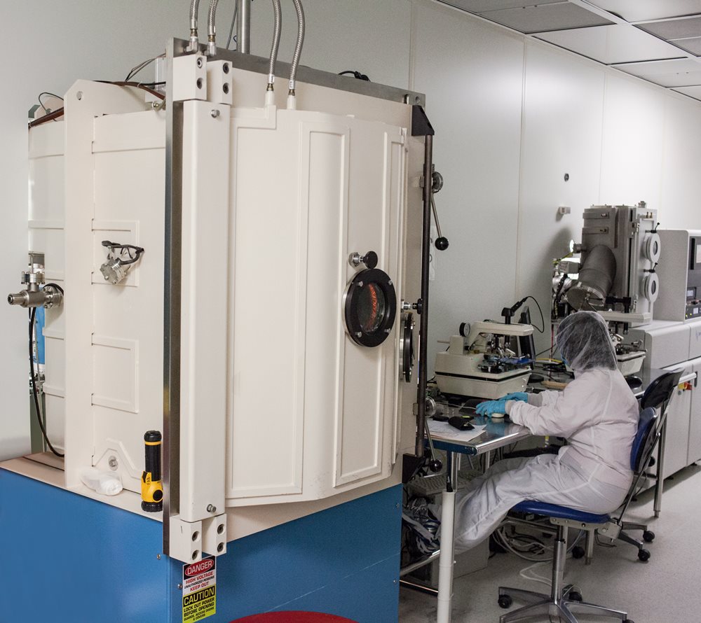
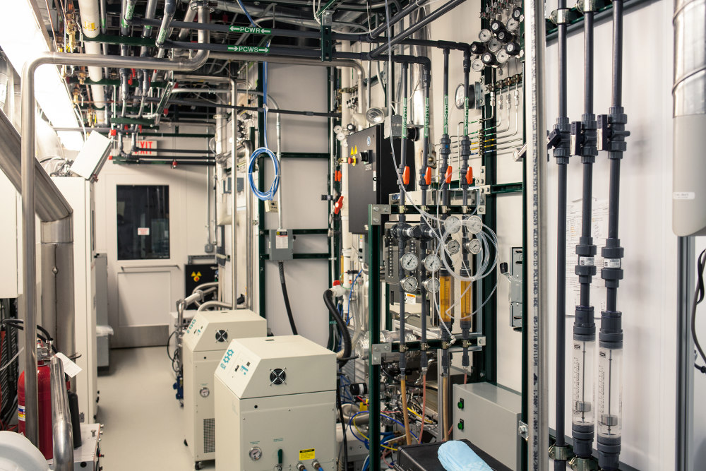
Wafer Fabrication
Our wafer fabrication facility (wafer fab) is designed for volume production of III-V semiconductor laser devices and LiNbO3 components as well as precision test targets and other select foundry operations. Our environmentally-controlled class 100/1000 cleanroom houses wafer fabrication processes such as epitaxial wafer growth, wafer bonding, photolithography, thin-film deposition, wet/dry etching, metal deposition, cleaving and optical facet coating.
Epitaxial Wafer Growth
Solid-source Molecular Beam Epitaxy (MBE) is used for III-V epitaxial wafer growth. MBE enables growth of complex multi-quantum well epitaxial structures with precise control of interface transitions as well as doping levels. We have in-house expertise to grow most III-V epitaxial structures that are comprised of the elements Ga, As, In, P, Al and Sb.
Click to Enlarge
Etch Bay
Device Fabrication
Capabilities
- Sub-Micron Photolithography
- Thin-Film Deposition: PECVD, Electron Beam Evaporation, RF Sputter Deposition
- Dry Etching: RIE and ICP
- Metal Deposition: E-beam Evaporation and Plating
- Thermal Processes: Diffusion, Rapid Annealing and Curing
- Cleaving and Dicing
- Optical Facet Coating: Anti-Reflection (AR) and High-Reflection (HR) Coatings
The wafer fabrication process consists of a sequence of controlled steps where material is either deposited or removed in patterns determined by the photolithography process. During photolithography, a protective "mask" is placed over certain areas of the device, which shields them from either etching or deposition. Etching is accomplished by exposing the wafer to a plasma or chemical that removes material. Deposition techniques include plasma-enhanced chemical vapor deposition (PECVD), RF sputter deposition, e-beam deposition and plating. Various furnaces are also used during the fabrication process for diffusion, annealing, planarization, wafer bonding and oxidation.
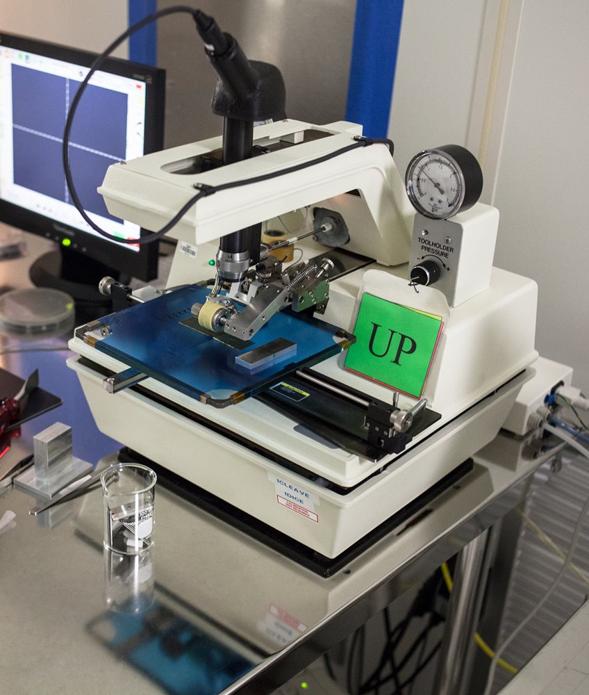
Click to Enlarge
Wafer Cleaving
Click to Enlarge
Ion Mill (Left) and Diffusion Furnaces (Right)
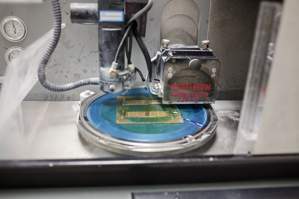
Cleaving/Dicing/Automated Handling
Semiconductor chips are fabricated with many individual devices on a single wafer. Wafers are first backside polished to reduce their thickness, making them easier to cleave. The wafer is then cleaved along crystal planes to create bars using automated scribe/break equipment. Each bar contains an array of many chips. Multiple bars are stacked and loaded into the optical coating chamber for application of precision facet coatings (see below). The coated bars are then diced and automated pick and place tools load the die onto carriers, where they can be easily transported for subsequent testing and packaging.
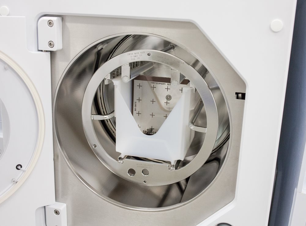
Optical Facet Coating
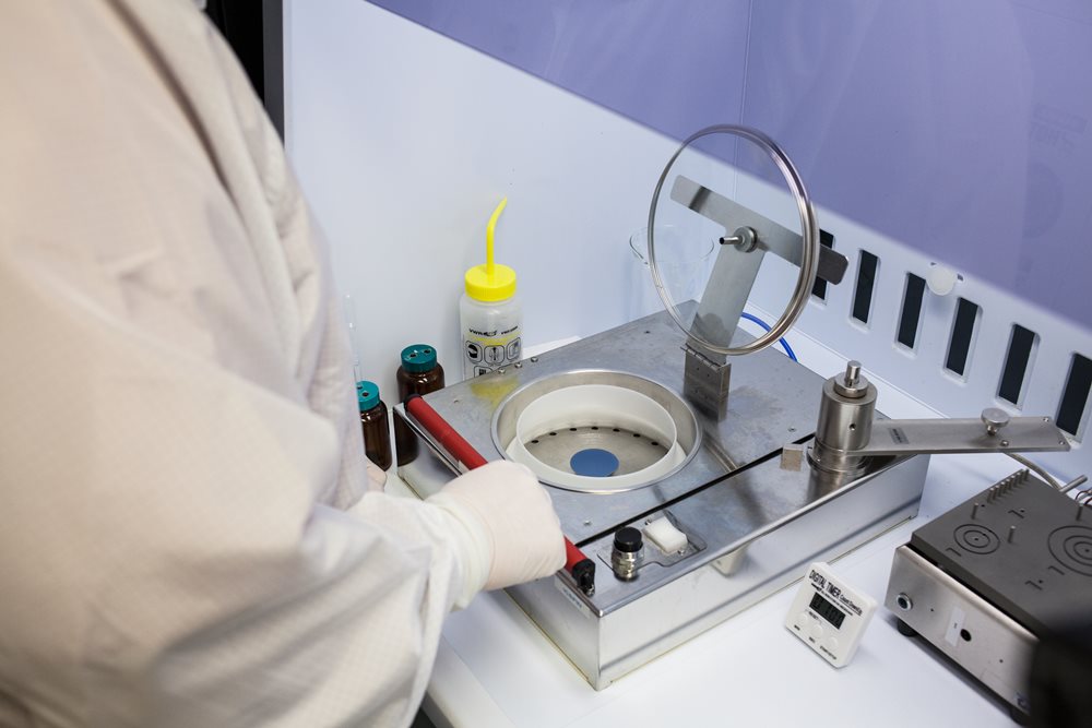
Semiconductors optical devices typically have one or more optical facets which are engineered to either reflect light back into the gain medium (to construct a laser cavity) or transmit light out of the gain medium without reflection (for example, in an optical amplifier). Optical coatings comprised of dielectric materials are deposited directly onto the device facets to enhance or reduce optical reflections. We have in-house optical monitoring capabilities that enable precision anti-reflection coatings that achieve reflectances of less than 0.03% over the C telecommunication band (1530 - 1565 nm). Our optical coatings are characterized by a multi-wavelength ellipsometer to accurately determine the thickness and refractive index of each layer.

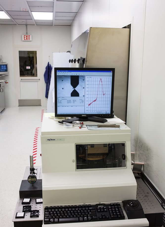
Click to Enlarge
Surface Profiler
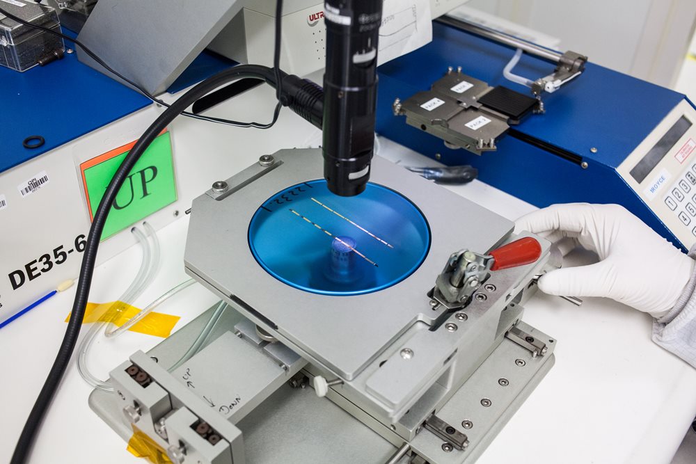
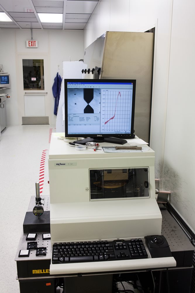
Metrology
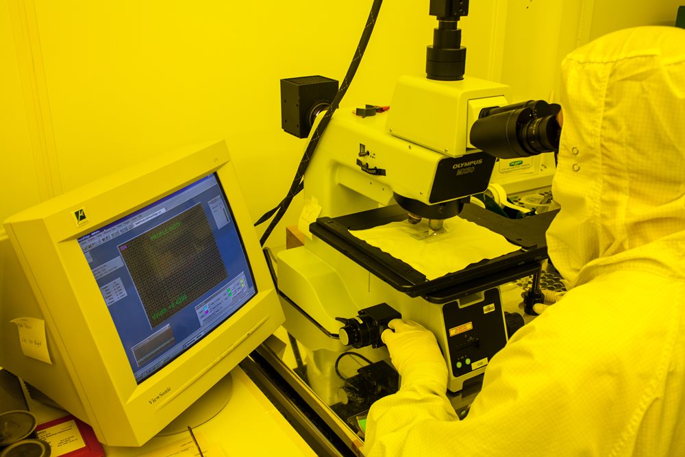
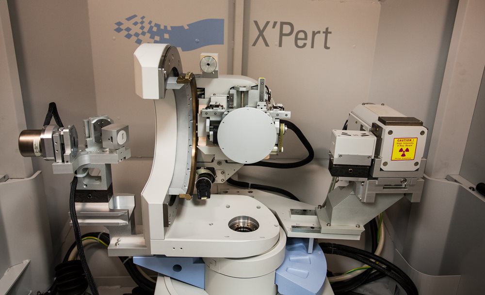
An important aspect of semiconductor device manufacturing is repeatability of all process steps. This requires constant monitoring with appropriate metrology to guarantee that the process remains within specifications. , Epitaxial wafer growth requires very specialized equipment and techniques to characterize the quality of the crystal growth using X-ray diffraction, photoluminescence intensity, electrochemical capacitance-voltage dopant profiling, and Hall-effect measurement of carrier mobility. Metrology tools used in the wafer fabrication process include a scanning electron microscope (SEM), surface profilometer, critical dimension (CD) optical microscope, reflectometer and ellipsometer.
For more information about our testing and quality capabilities, including testing for finished devices, see the Testing & Quality tab above.

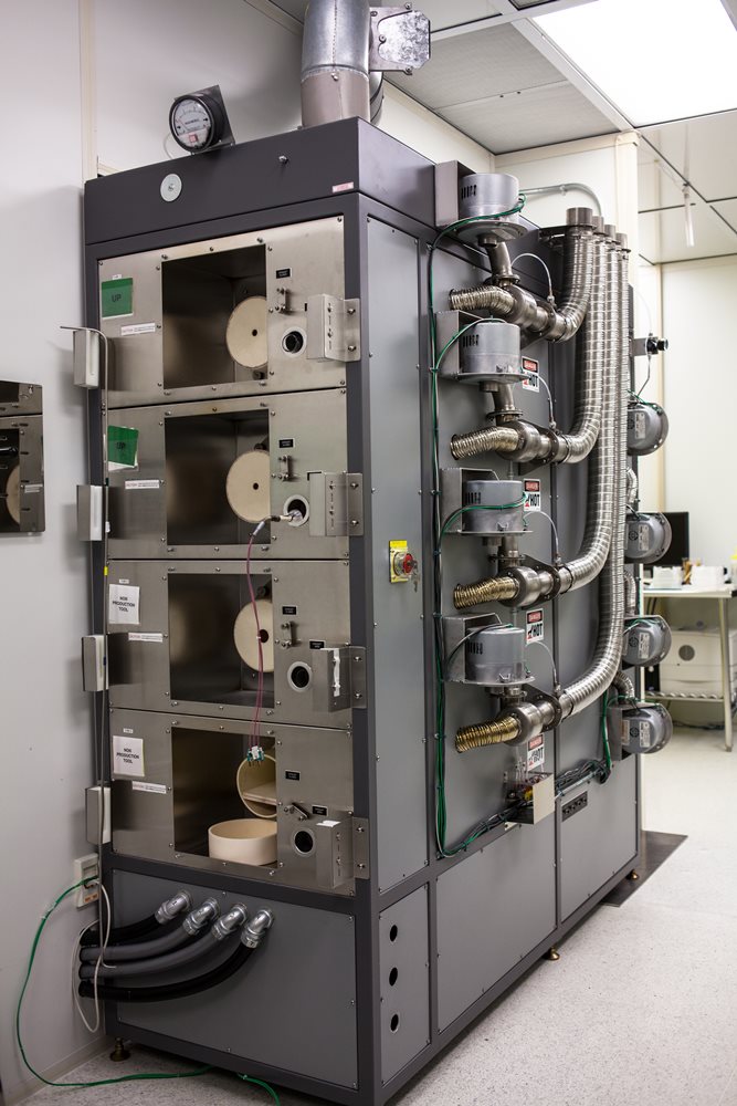

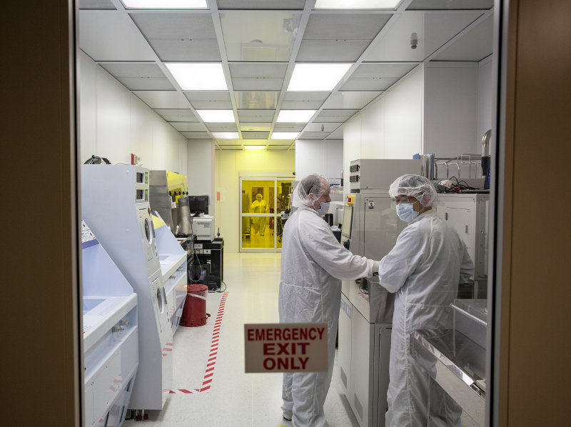
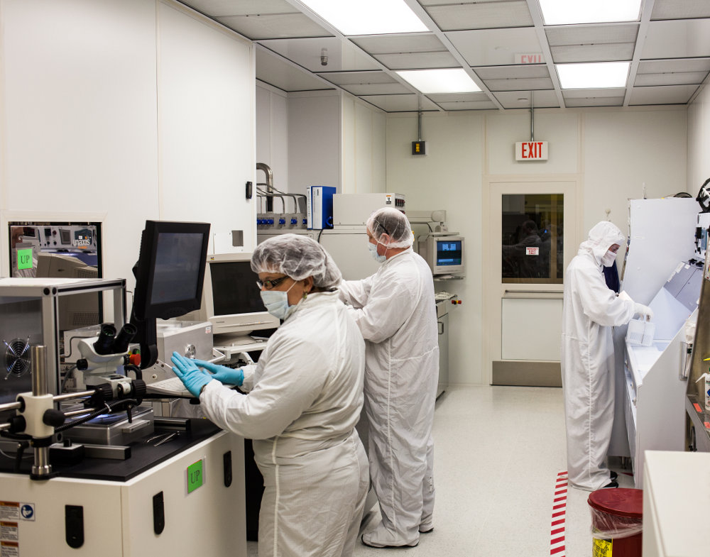
Click to Enlarge
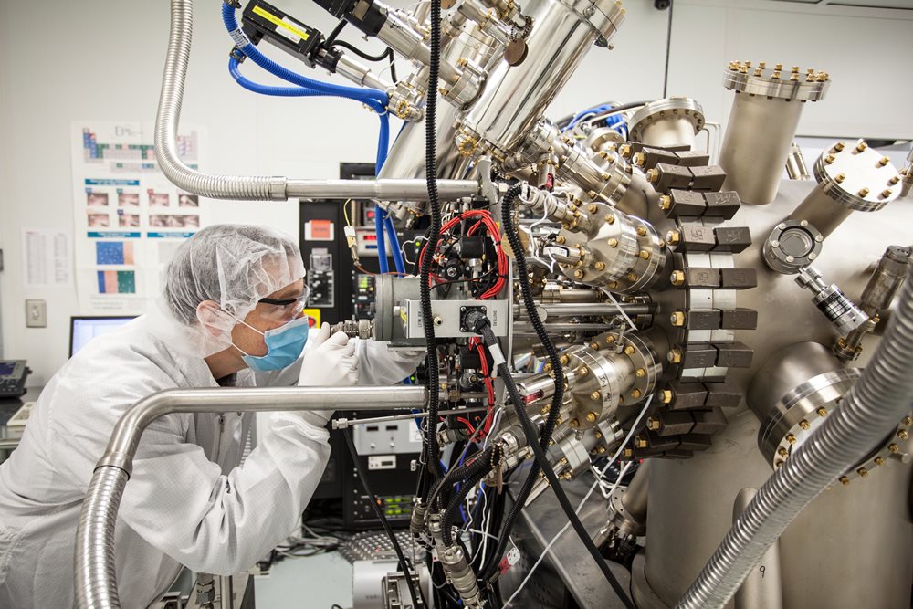
Class 1000 Cleanroom Area for Wafer Packaging, Inspection, and Testing
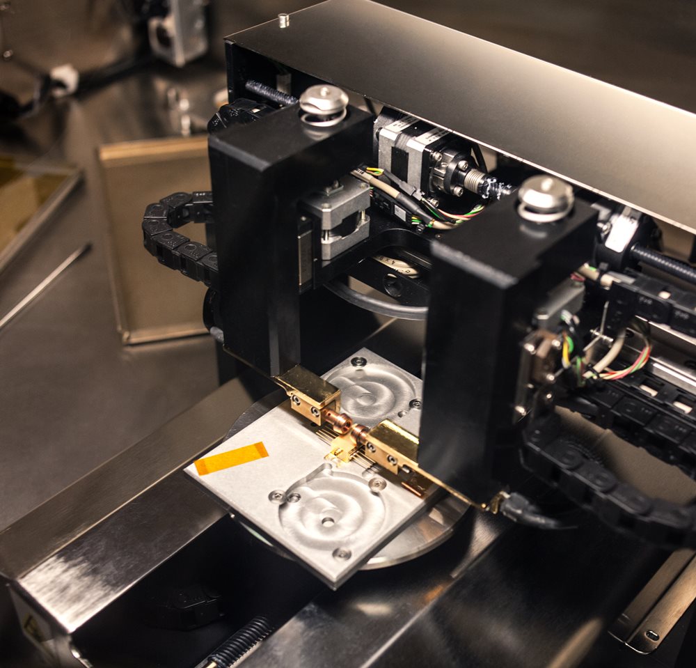
Packaging
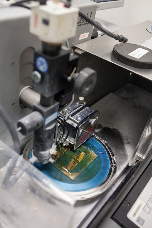
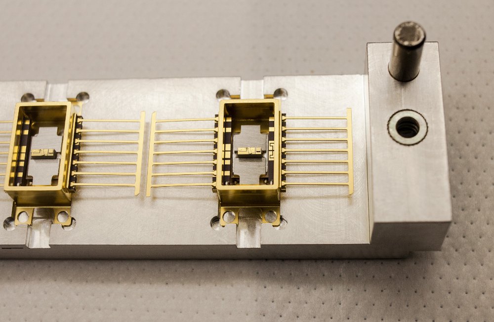
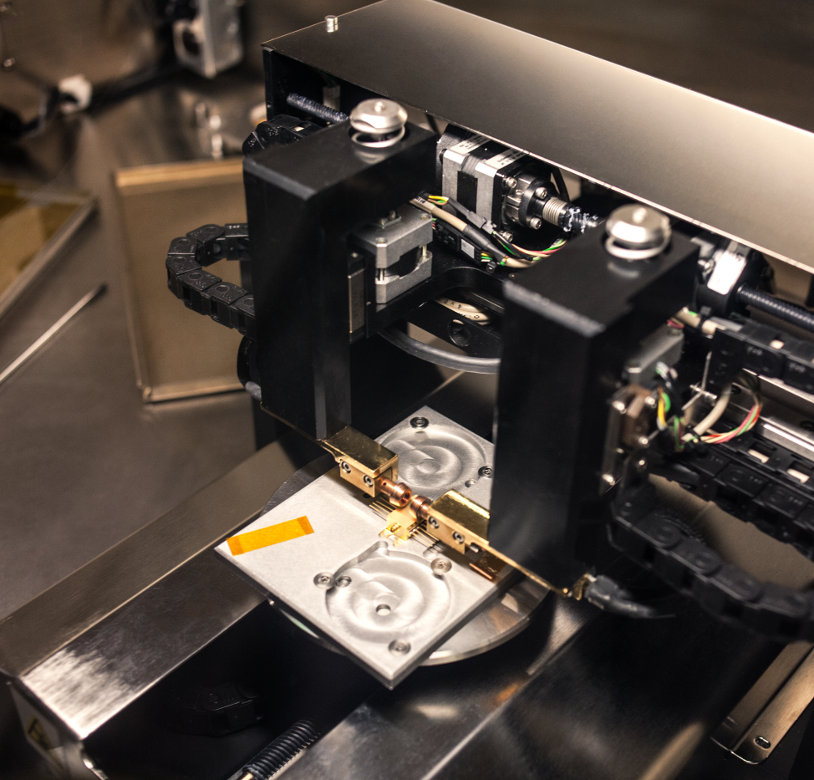
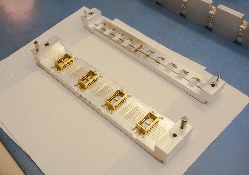
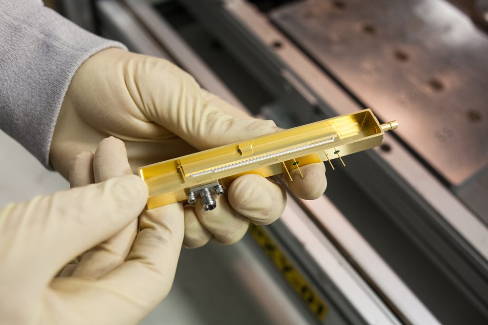
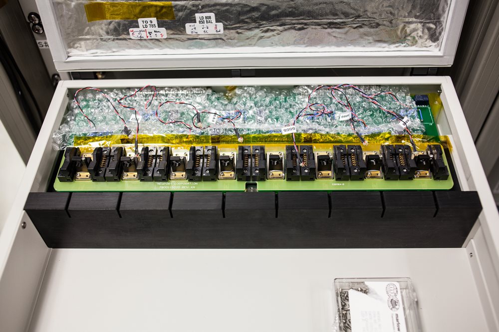
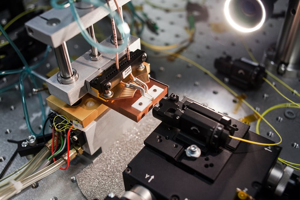
The semiconductor and LiNbO3 dies produced by the wafer fab are available in a wide variety of opto-electronic package types. This packaging is done in our class 10,000 assembly areas (shown to the right). The simplest packages are chip-on-submount (CoS) or open heatsink sink designs such as a C-mount or TO-header. These provide direct access to the semiconductor laser facet. Another very popular format for laser diodes is the TO-can with hermetically sealed window cap and monitor photodiode. We produce several different types of fully fiber-coupled products including industry-standard 14-pin butterfly and LiNbO3 modulator packages, as well as 6-pin half butterfly and pigtailed TO-cans.

Click to Enlarge
Wire Bonding a Quantum Cascade Laser on a C-Mount
Click to Enlarge
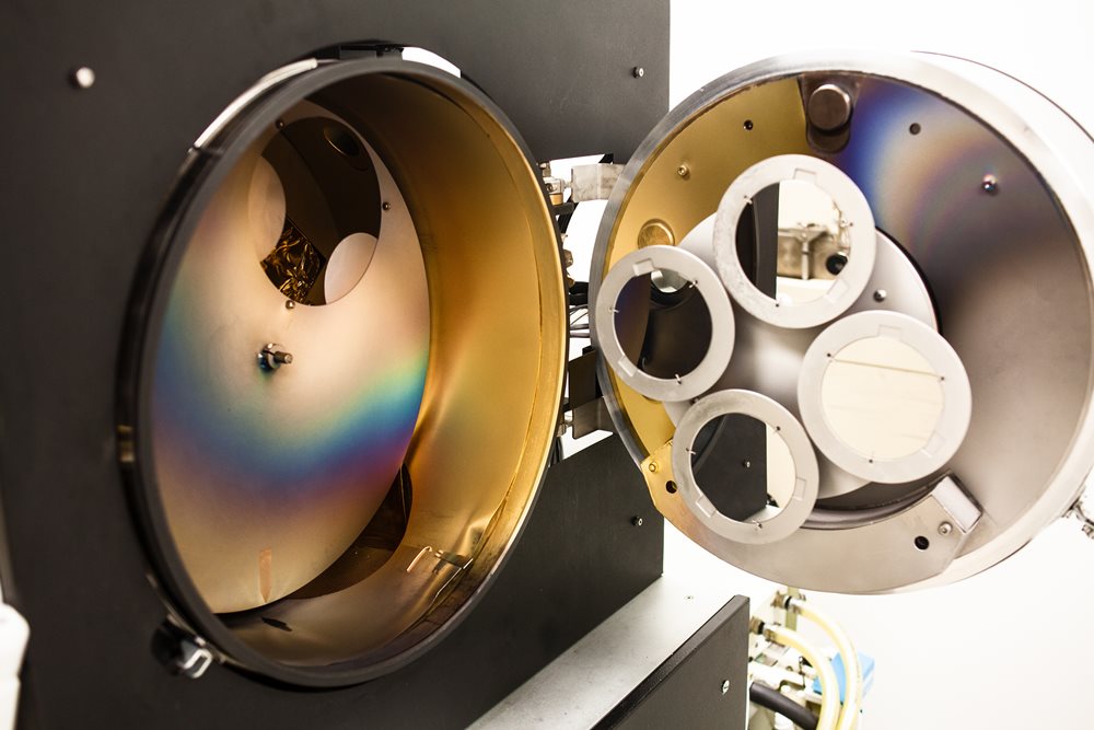
Two Butterfly Packages shown with Optical Amplifier Chips Mounted Inside
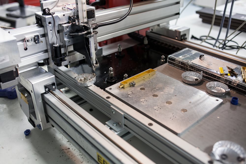
Die Bonding and Wire Bonding
- Die Bonding: Precision Placement and Solder Attachment of Chips
- Wire Bonding: Manual Ball and Wedge Bonding of Wire Leads
The process of packaging begins with die bonding, which is the attachment the semiconductor chip to a ceramic submount. The submount is -designed for efficient heat removal and proper coefficient of thermal expansion (CTE) match to the semiconductor material. Our automated and manual die bonding machines allow for precise die bonding in both epi-side up and epi-side down chip configurations.
After the die bonding process, electrical contact is made to the chip by bonding gold wires from the top of the chip to bond pads located on the submount. The size and number of the wire bonds depends on the device, operating current, and operating frequency.
Chip-on-Submount (CoS) level devices can be fully tested and burned in without further packaging. We supply CoS devices for both large volume OEM applications as well as stock chip-on-submount products.
Click to Enlarge
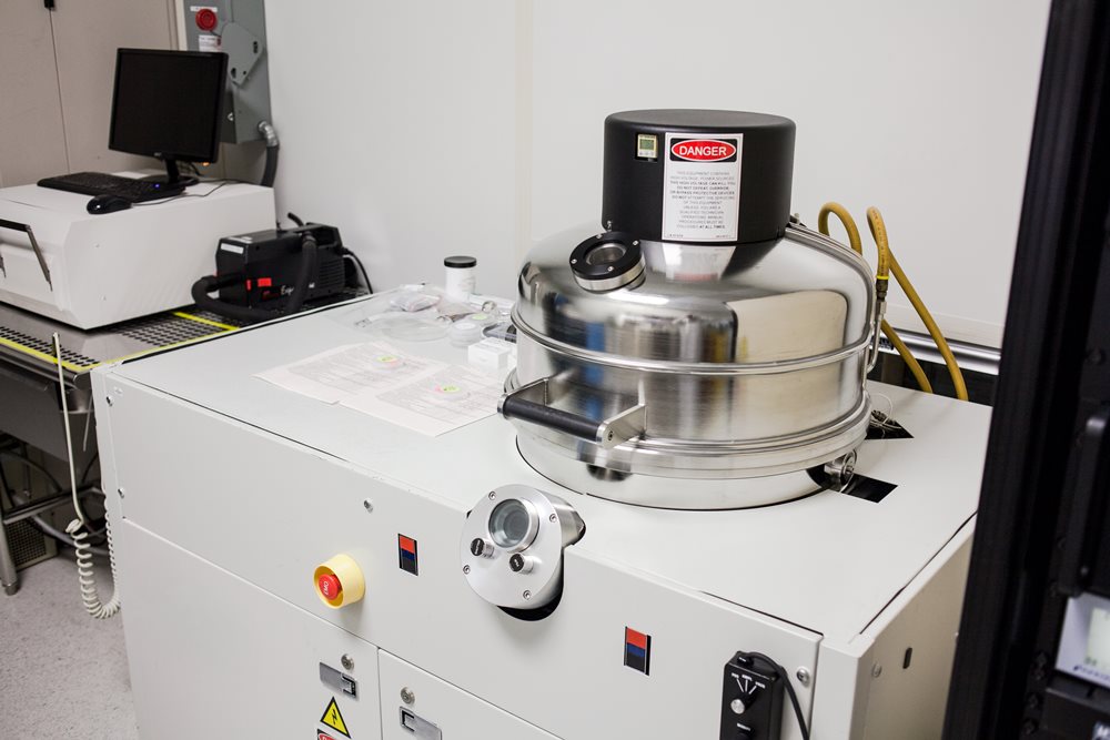
Laser Welding Apparatus
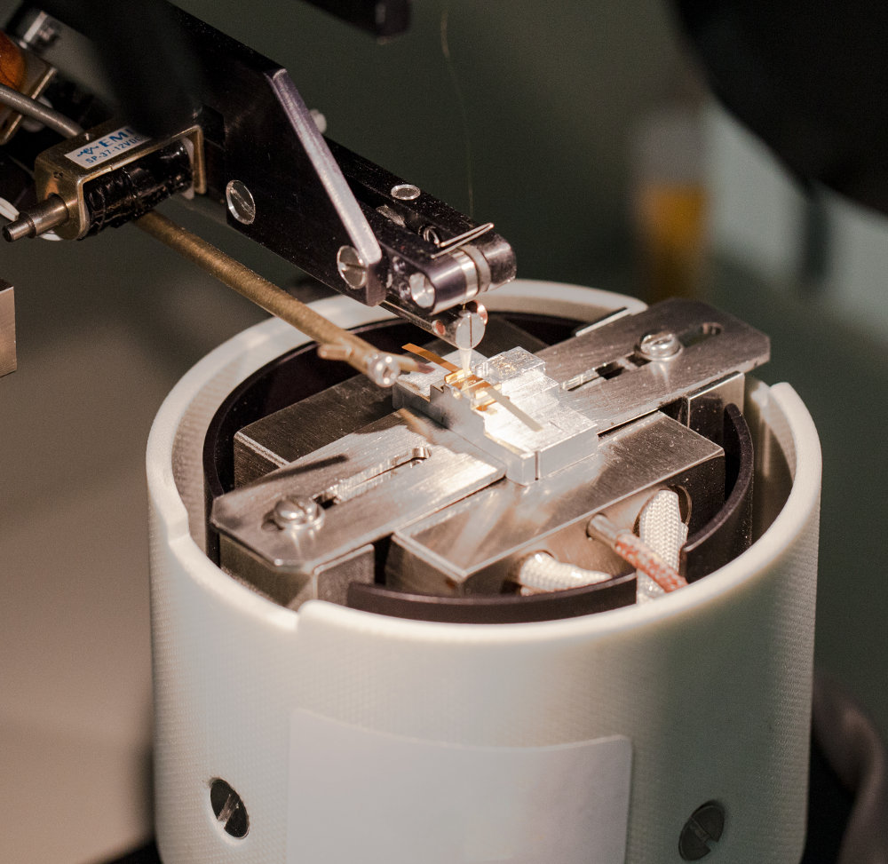
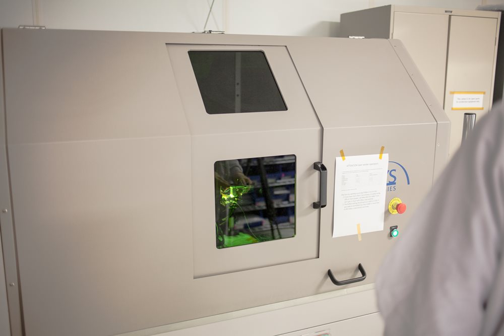
Laser Welding
- Precise Alignment and Welding of Optical Elements within a Semiconductor Package
Laser welding is a well-established process in the opto-electronic packaging industry for precision attachment of optical components within a sub-assembly. High energy laser pulses enable rapid welding of material surfaces with minimal post-weld shift of the optical components as well as excellent long-term mechanical stability. Our proprietary laser welding processes are used in all butterfly-packaged products including single-ended devices (i.e. SLDs and FP lasers), double-ended devices (i.e. SOA and BOA) and half-butterfly devices (gain chips).
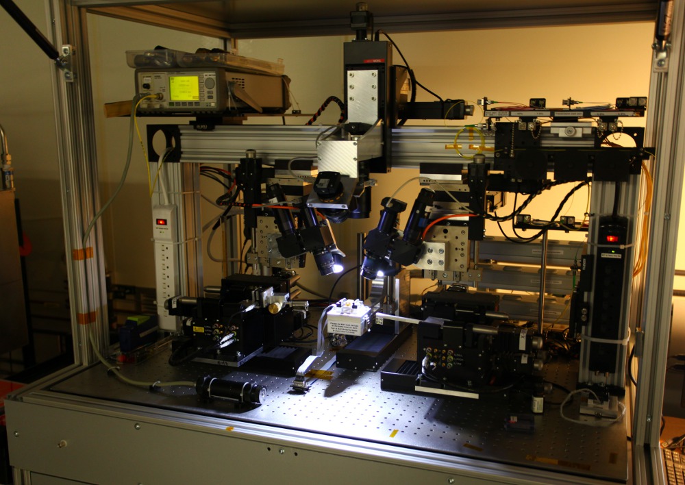
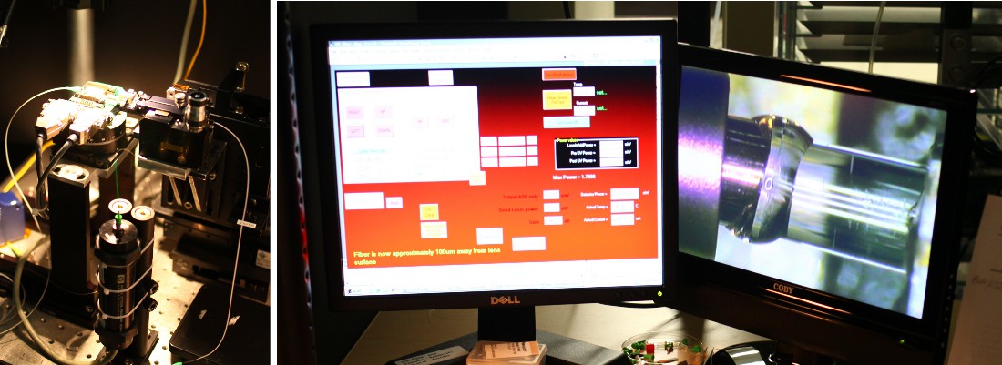
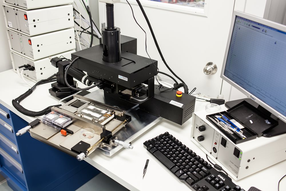
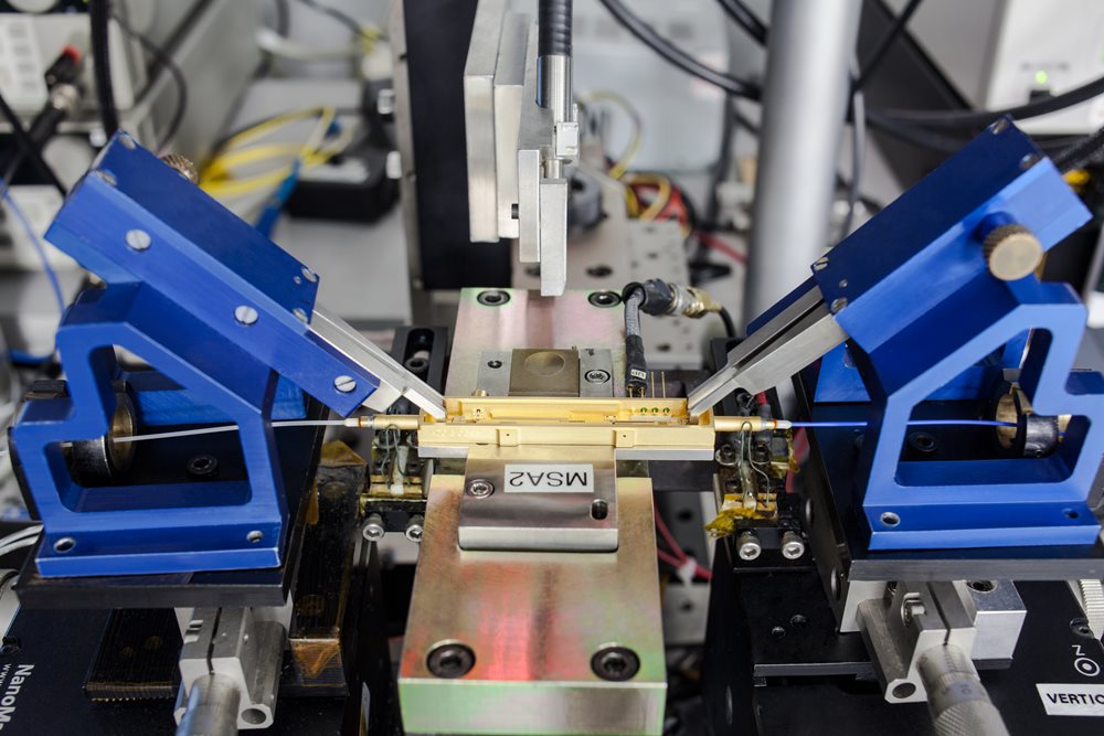
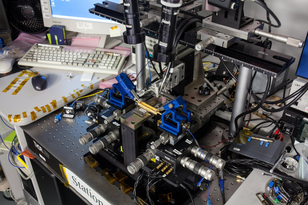
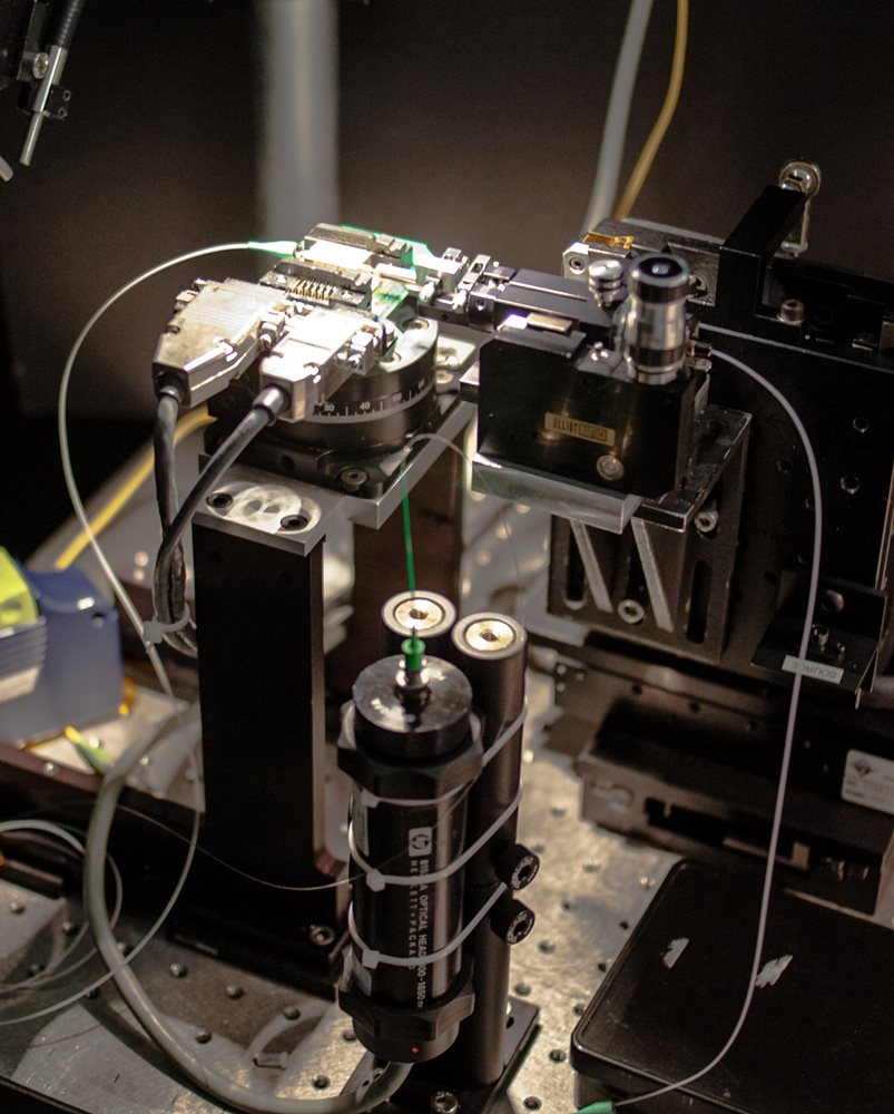
Fiber Pigtailing
- Manual and Automatic Fiber Pigtailing Stations
Our butterfly packages use a transfer lens design to efficiently couple light from the semiconductor chip to the optical fiber. This approach enables optical isolators and/or other components to be incorporated inside the butterfly package. Our LiNbO3 modulators use a direct butt-coupled design where the optical fiber is directly attached to the modulator chip. Both package types have been qualified to GR-468 CORE Telcordia requirements and have been deployed world-wide in demanding OEM applications in telecom, medical, defense, and industrial markets.
Hermetic Sealing
- Provides Reliability under a Variety of Environmental Conditions
Semiconductor and LiNbO3 devices are particularly sensitive to humidity and environmental changes. Hermetic sealing is very important for long-term stability and reliability. Our butterfly packages, TO-cans, and LiNbO3 fiber-coupled modulators are hermetically sealed in a dry-nitrogen atmosphere, providing a benign environment for the active chip component. The hermetic seal is created using electrical resistance welding to attach the lid to the package frame. This seal prevents atmospheric conditions from influencing device performance.
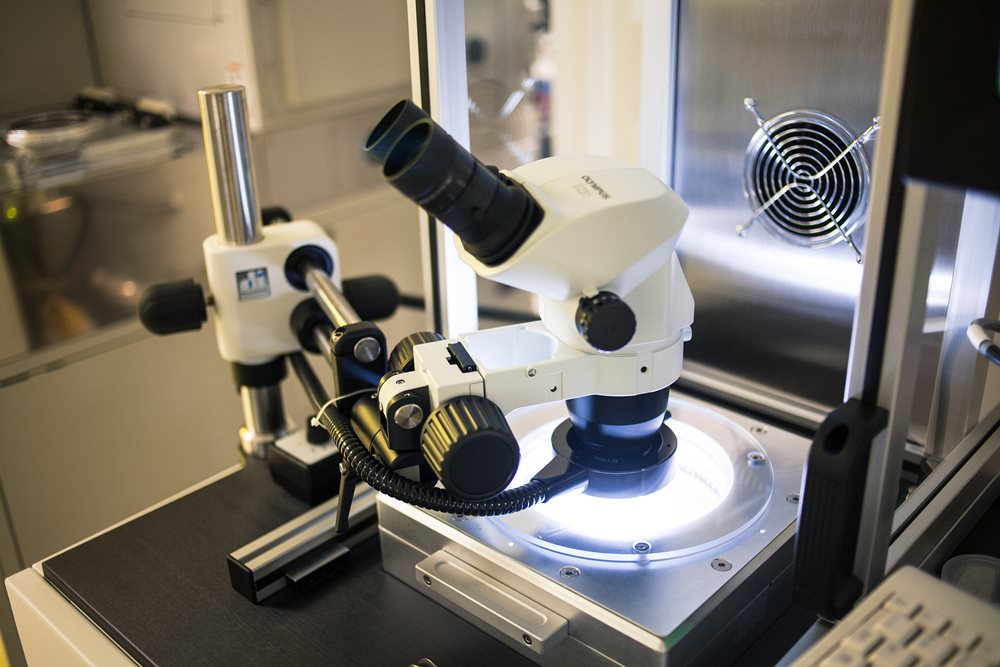
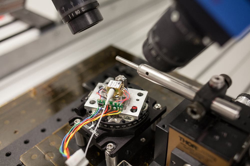
Click to Enlarge
Pigtailing Equipment (Left) and Alignment Monitors (Right)
Click to Enlarge
Hermetically Sealing a Butterfly Package
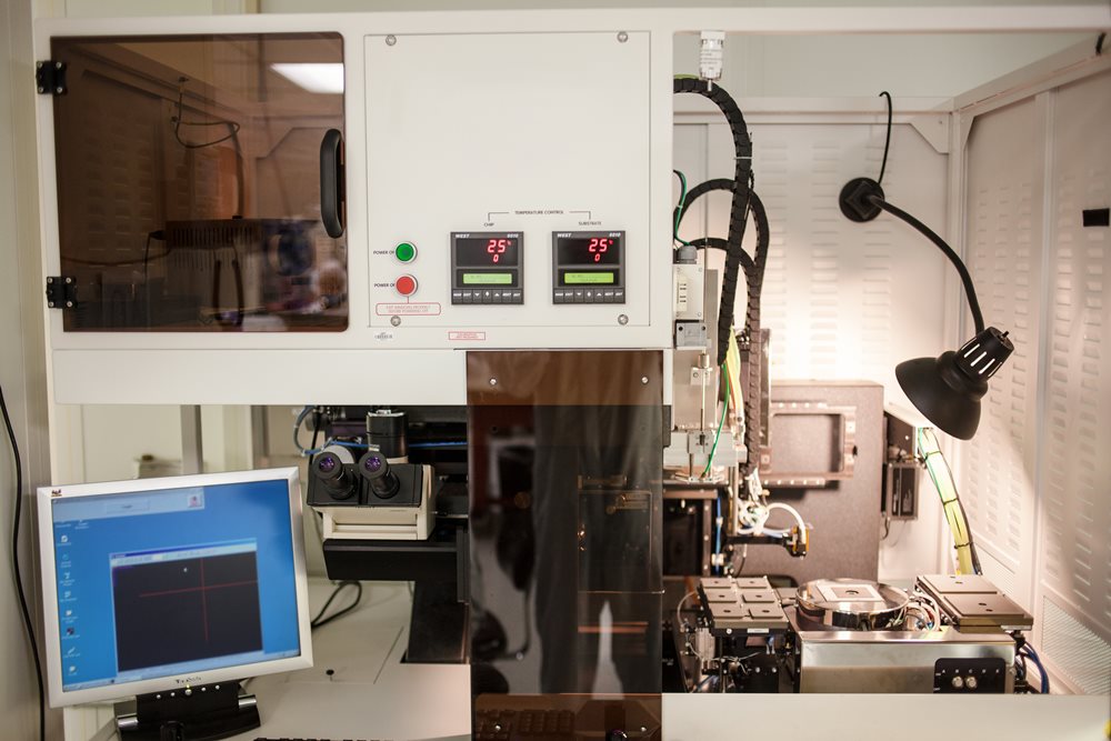


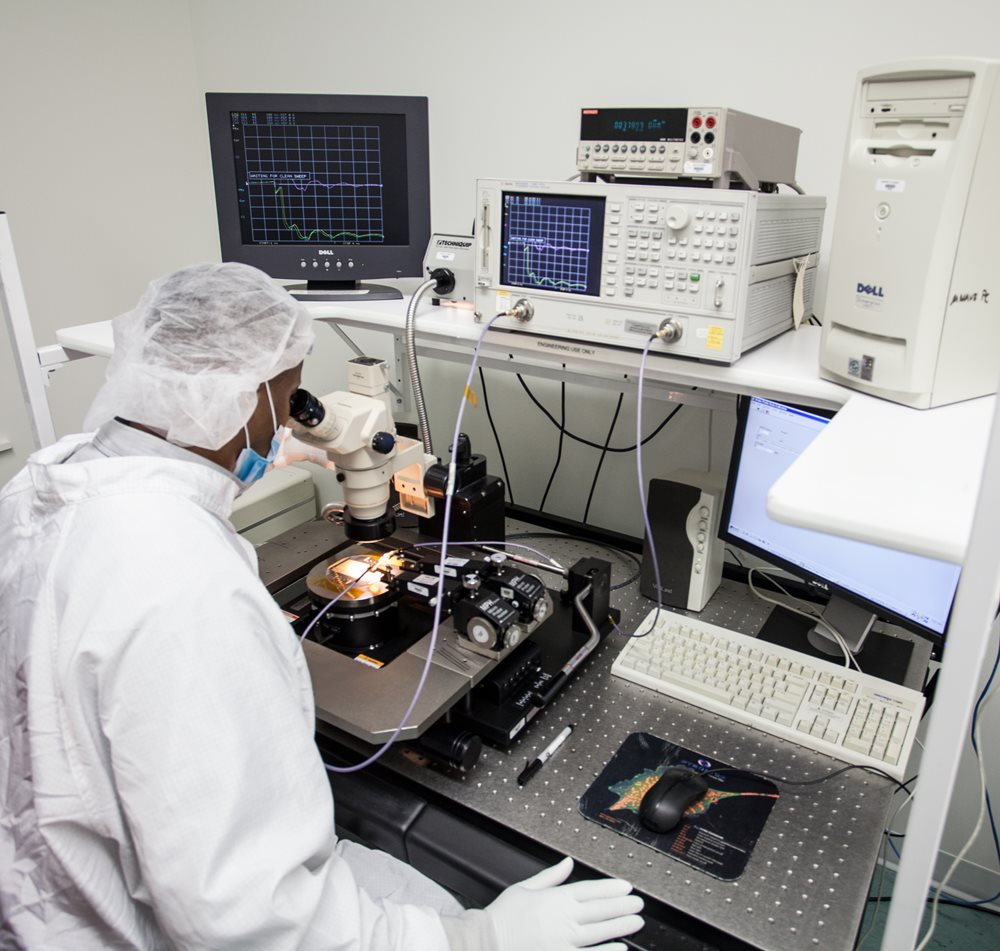
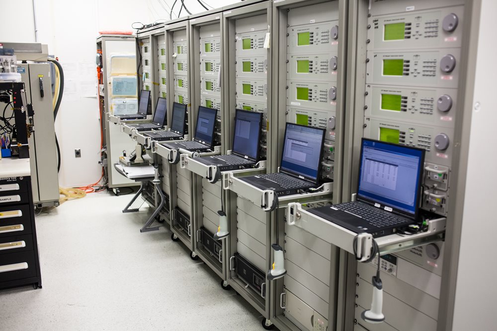
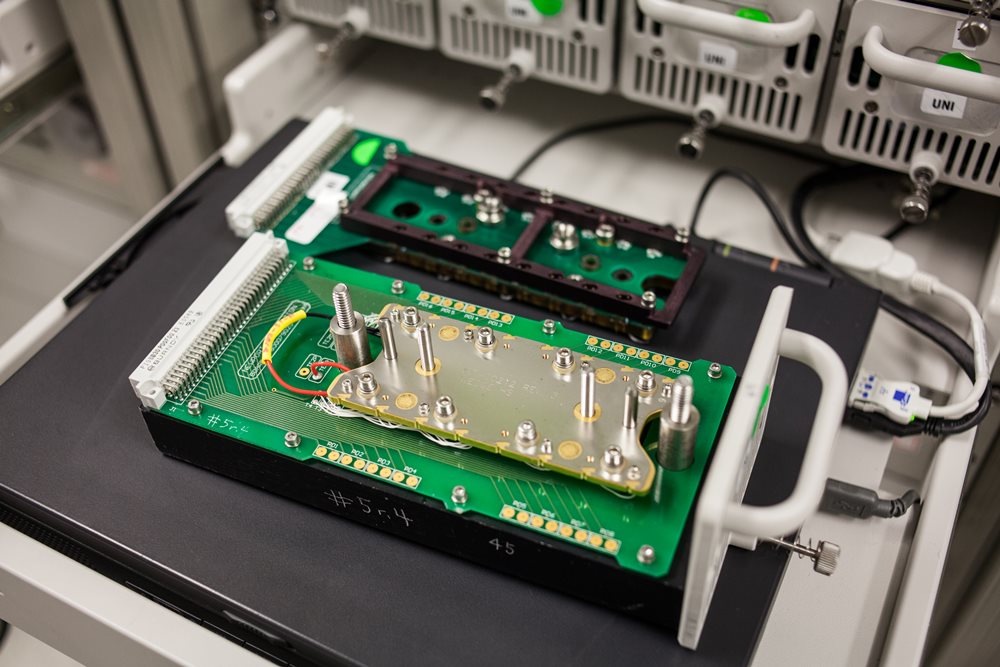
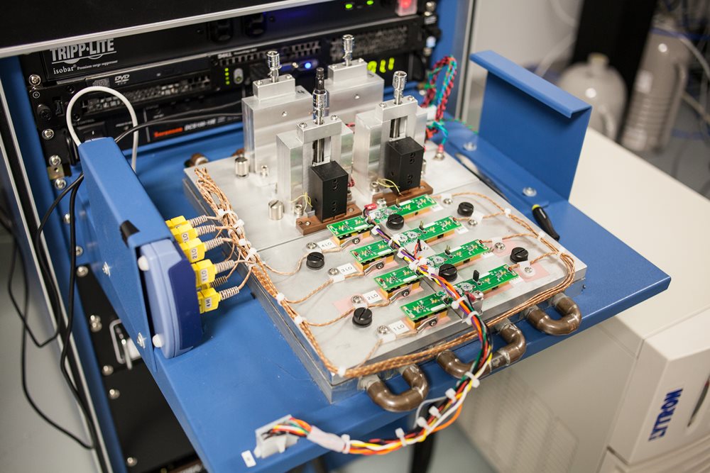
Testing and Quality
Test Capabilities
- Performance Testing and Device Characterization
- CW and Pulsed Output Power
- Spectral Characteristics: Wavelength, Optical Bandwidth, Spectral Ripple, Side-Mode-Suppression Ratio (SMSR)
- CW and Pulsed Far Field
- External Cavity Laser Parameters
- RIN and Linewidth
- Frequency Response to 40 GHz
- Bit-Error-Rate (BER) and Chirp
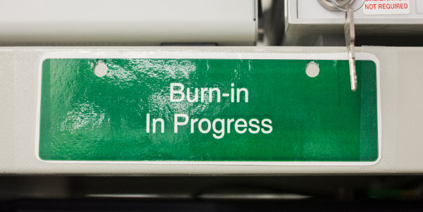
- Burn-In Testing
- Reliability Testing
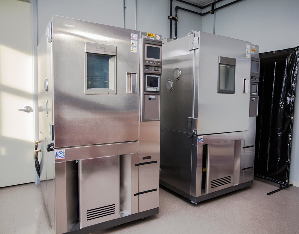
- Environmental Testing
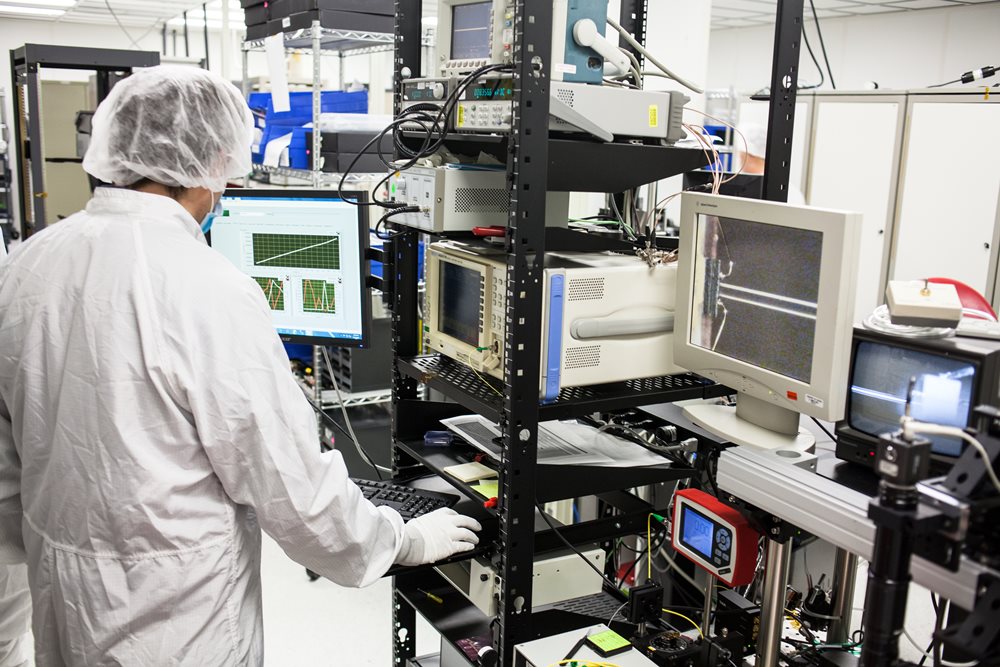
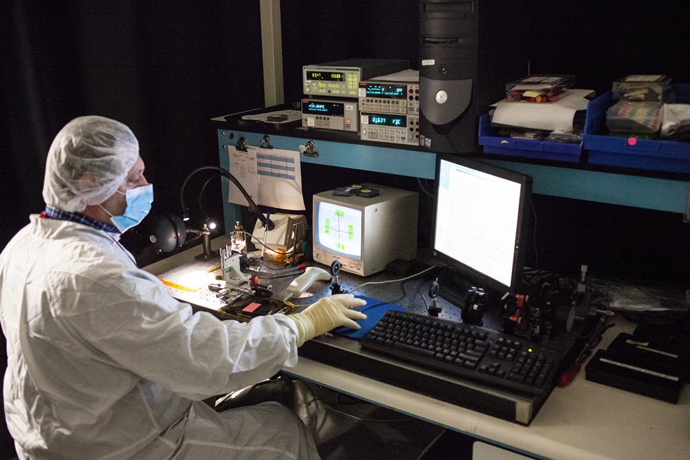
Thorlabs has extensive testing capabilities for final testing of high-volume production parts as well as rigorous reliability/environmental testing. We burn-in and measure the optical characteristics of all chip-on-submount, TO-can, butterfly, and modulator products for both catalog and OEM sales. For new products or ongoing quality/re-qualification of existing products, we have in-house capability for temperature cycling and high/low temperature storage, as well as long-term accelerated aging. Our engineering team is experienced in developing and qualifying products for the telecommunications, medical, and defense industries.


OEM and Custom Ordering Information
We offer both catalog and OEM/custom products at all levels of assembly, including chip on submount (CoS), heatsink, and fiber-coupled packages, as well as complete sub-systems with integrated control electronics. Our design team can engineer a full range of custom solutions completely in house, including custom chips, optical coatings, and packaging. Contact Sales-TQE@thorlabs.com to consult with our engineering team regarding a custom product.

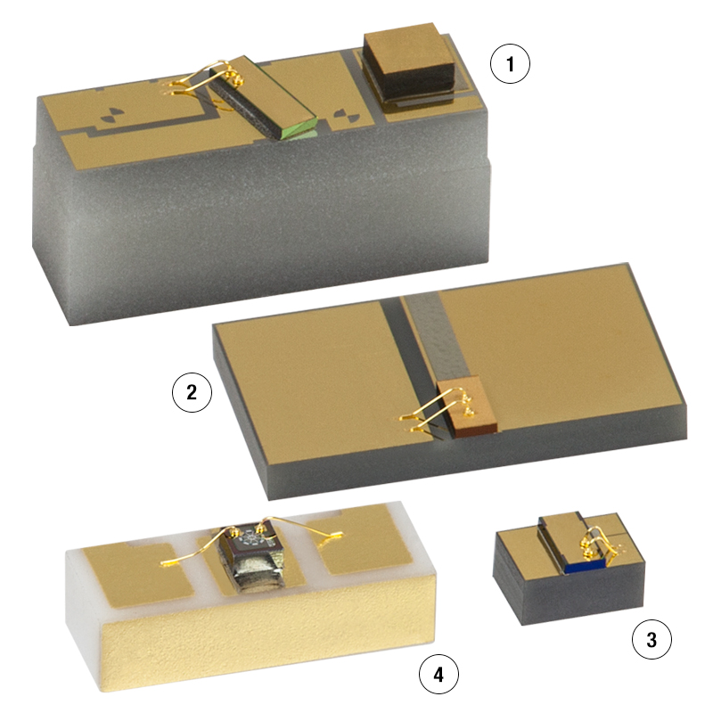
Click to Enlarge
Various Chip-on-Submount Level Devices, Including an Optical Amplifier (1), a Fabry-Perot Laser (2), a Single Angled Facet Gain Chip (3) and a VCSEL Laser (4). The field of view is approximately 1 cm wide, and all chips are shown to scale.

Click to Enlarge
Butterfly-Packaged Fabry-Perot Laser
Timeline
|

Beginnings of Thorlabs Quantum Electronics
Since 2009, Thorlabs Quantum Electronics (TQE) has operated in Jessup, Maryland, as our first and primary semiconductor foundry. TQE's key personnel began working in the industry in 1998 under the name of Quantum Photonics.
Quantum Photonics, Inc.® (QPI) was founded in order to commercialize advanced semiconductor laser technology pioneered at the University of Maryland. Initially focused on telecommunications applications, QPI quickly attracted venture capital investments, enabling the company to establish a comprehensive, vertically integrated manufacturing facility that included III-V epitaxial wafer growth, wafer fabrication, and optoelectronics packaging.
In 2003, QPI merged with Codeon Corporation, thereby adding high-speed lithium niobate modulators to its manufacturing capabilities. The combined entity was known as Covega Corporation. Covega established itself as a leading supplier of semiconductor laser gain devices and lithium niobate modulators, creating key products for the medical, industrial, and defense markets.
In 2009, Thorlabs acquired the Covega manufacturing facility, forming TQE. TQE is a highly active division of Thorlabs, and has continued to add products to its manufacturing portfolio, including NIR GaAs laser diodes, state-of-the-art MEMS-tunable VCSELs, and the market's leading selection of MIR quantum cascade lasers and interband cascade lasers (QCLs and ICLs). Having accumulated over 10 billion device hours on its telecom gain chips without a single failure in the field, TQE provides Thorlabs with the means to develop, manufacture, and support leading-edge optoelectronic components for the R&D community, as well as the ability to serve as a flexible, vertically integrated partner for OEM customers.
| Posted Comments: | |
进一 严
(posted 2020-11-06 16:59:17.833) 广泛的外延晶圆设计、机械设计(Solidworks)、光学设计(Zemax)、温度模型(Comson)和电子设计(Altium)能力。这里面的comson是个什么软件? YLohia
(posted 2020-11-06 09:44:02.0) Thank you for contacting Thorlabs. An applications engineer from our team in China (techsupport-cn@thorlabs.com) will contact you directly. |