Pinhole Wheels
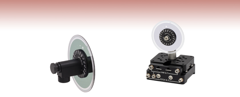
- 16-Position Pinhole Wheel with Hole Sizes from Ø25 µm to Ø2 mm
- Lithographically Etched Chrome on Glass
- AR Coated for 350 - 700 nm on Both Sides
Application Idea
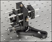
A PHWM16 Pinhole Wheel Post Mounted to a PY005 5-Axis Translation Stage for Alignment
PHWM16
Mounted 16-Position Pinhole Wheel

Please Wait
Click to Enlarge
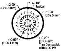
Figure 1.1 The inner ring is engraved with pinhole sizes and alignment marks.
Features
- Wheel with 16 Lithographically Etched Pinholes (Transparent Glass)
- Pinhole Sizes from Ø25 µm to Ø2 mm
- Ø2.00" (Ø50.8 mm), 0.02" (0.5 mm) Thick Chrome-Plated Borosilicate Substrate
- Includes the NDC-PM Post Mount Assembly (See the Assembly Tab for Mounting Instructions)
- AR Coated for 350 - 700 nm on Both Sides (Ravg < 0.5%)
The pinhole wheel is comprised of borosilicate glass disks that are chrome-plated on one side with 16 lithographically etched pinholes ranging from Ø25 µm to Ø2 mm. The radially positioned pinholes enable a user to test multiple pinhole sizes within their experiment and require only minor alignment after each rotation. Additionally, Thorlabs also offers motorized pinhole wheels designed for confocal microscopy systems.
The Ø2.00" (Ø50.8 mm), 0.02" (0.5 mm) thick disks are manufactured using photolithography; therefore, the pinholes are formed from the transparent substrate material where the chrome plating has been chemically etched away. Both sides of the wheel are AR coated for 350 - 700 nm (Ravg < 0.5%) to increase transmission through the wheel. The Delrin®* inner disc is engraved with the pinhole sizes and alignment marks that point towards the pinholes. See Figure 1.1 and Table 1.2 for pinhole sizes and positions.
The included NDC-PM Post Mount Assembly allows the pinhole wheel to be mounted to a rotating axle that can be threaded onto any Thorlabs Ø1/2" Post. Adapters for both 8-32 and M4 mounting holes are included with each mount. The shaft of the mount can be locked by tightening the side-located setscrew using the included 0.05" (1.3 mm) hex key. Assembly of the mount is required and instructions for mounting the pinhole wheel to a NDC-PM are provided in the Assembly tab.
*Delrin® is a registered trademark of DuPont Polymers, Inc.
| Table 1.2 Pinhole Specifications | |||||
|---|---|---|---|---|---|
| Positiona | Pinhole Size | Position | Pinhole Size | Position | Pinhole Size |
| A | Ø100 µm with Ø50 µm Obstruction | G | Ø50 µm | M | Ø125 µm |
| B | Ø25 µm | H | Ø60 µm | N | Ø200 µm |
| C | Ø30 µm | I | Ø70 µm | O | Ø300 µm |
| D | Ø35 µm | J | Ø80 µm | P | Ø1000 µm |
| E | Ø40 µm | K | Ø90 µm | Q | Ø2000 µm |
| F | Ø45 µm | L | Ø100 µm | - | - |
Click to Enlarge
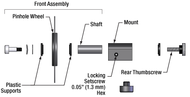
Figure 2.1 Exploded Schematic of PHWM16
Mounting the Pinhole Wheel
The 16-position pinhole wheel can be post mounted using the included NDC-PM Post Mount Assembly by following the assembly steps below. Adapters for both 8-32 and M4 mounting holes are included.
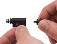
- Tighten the 4-40 locking setscrew on the side of the NDC-PM assembly using the included 0.05" (1.3 mm) hex key to lock the shaft in position. Unscrew and remove the rear thumbscrew, then loosen the locking setscrew (Figure 2.2).
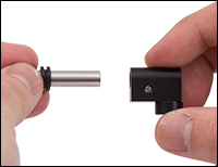
- Pull the front assembly from the mount (Figure 2.3).
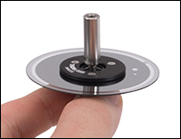
- While holding the assembly vertically unscrew the shaft. Remove the top plastic support and place the pinhole wheel with the engraving facing down. Then, secure the pinhole wheel by placing the plastic support in position and screwing the shaft onto the cap screw (Figure 2.4).
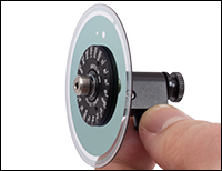
- Insert the front assembly with pinhole wheel into the mount, lock the locking setscrew, and then screw on the rear thumbscrew (Figure 2.5).
During installation and use, the guidelines below may be helpful:
- Holding the mount vertically (see Figure 2.4) prevents the components (e.g., washer, spacer, and plastic supports) from falling apart during assembly.
- Use light force when securing the pinhole wheel as overtightening may cause the wheel to crack.
- The wheel may still rotate if moved by hand even if the locking setscrew is fully tightened.
Click to Enlarge
Figure 2.2 Lock the Mount and Remove the Rear Thumbscrew
Click to Enlarge
Figure 2.3 Unlock the Mount and Pull the Front Assembly Out of the Mount
Click to Enlarge
Figure 2.4 Hold Vertically and Secure the Pinhole Wheel
Click to Enlarge
Figure 2.5 Insert the Front Assembly into the Mount and Screw on the Rear Thumbscrew
Principles of Spatial Filters
For many applications, such as holography, spatial intensity variations in the laser beam are unacceptable. Our KT311 spatial filter system is ideal for producing a clean Gaussian beam.
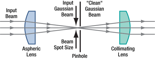
Figure 3.1 Spatial Filter System
The input Gaussian beam has spatially varying intensity "noise". When a beam is focused by an aspheric lens, the input beam is transformed into a central Gaussian spot (on the optical axis) and side fringes, which represent the unwanted "noise" (see Figure 3.2). The radial position of the side fringes is proportional to the spatial frequency of the "noise".
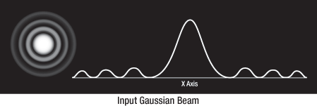
Figure 3.2 Input Gaussian Beam
By centering a pinhole on a central Gaussian spot, the "clean" portion of the beam can pass while the "noise" fringes are blocked (see Figure 3.3).
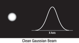
Figure 3.3 Clean Gaussian Beam
The diffraction-limited spot size at the 99% contour is given by:

where λ = wavelength, ƒ=focal length and r = input beam radius at the 1/e2 point.
Choosing the Correct Optics and Pinhole for Your Spatial Filter System
The correct optics and pinhole for your application depend on the input wavelength, source beam diameter, and desired exit beam diameter.
For example, suppose that you are using a 650 nm diode laser source that has a diameter (1/e2) of 1.2 mm and want your beam exiting the spatial filter system to be about 4.4 mm in diameter. Based on these parameters, the C560TME-B mounted aspheric lens would be an appropriate choice for the input side of spatial filter system because it is designed for use at 650 nm, and its clear aperture measures 5.1 mm, which is large enough to accommodate the entire diameter of the laser source.
The equation for diffraction limited spot size at the 99% contour is given above, and for this example, λ = (650 x 10-9 m), f = 13.86 mm for the C560TM-B, and r = 0.6 mm. Substitution yields

Diffraction-Limited Spot Size (650 nm source, Ø1.2 mm beam)
The pinhole should be chosen so that it is approximately 30% larger than D. If the pinhole is too small, the beam will be clipped, but if it is too large, more than the TEM00 mode will get through the pinhole. Therefore, for this example, the pinhole should ideally be 19.5 microns. Hence, we would recommend the mounted pinhole P20D, which has a pinhole size of 20 μm. Parameters that can be changed to alter the beam waist diameter, and thus the pinhole size required, include changing the input beam diameter and focal length of focusing lens. Decreasing the input beam diameter will increase the beam waist diameter. Using a longer focal length focusing lens will also increase the beam waist diameter.
Finally, we need to choose the optic on the output side of the spatial filter so that the collimated beam's diameter is the desired 4.4 mm. To determine the correct focal length for the lens, consider the following diagram in Figure 3.4, which is not drawn to scale. From the triangle on the left-hand side, the angle is determined to be approximately 2.48o. Using this same angle for the triangle on the right-hand side, the focal length for the plano-convex lens should be approximately 50 mm.

Figure 3.4 Beam Expansion Example
For this focal length, we recommend the LA1131-B plano-convex lens [with f = 50 mm at the design wavelength (λ = 633 nm), this is still a good approximation for f at the source wavelength (λ = 650 nm)].
Note: The beam expansion equals the focal length of the output side divided by the focal length of the input side.
For optimal performance, a large-diameter aspheric lens can be used in place of a plano-convex lens if the necessary focal length on the output side is 20 mm (see AL2520-A, AL2520-B, AL2520-C). These lenses are 25 mm in diameter and can be held in place using the supplied SM1RR Retaining Ring.
| Table 4.1 Damage Threshold Specifications | |
|---|---|
| Item # | Damage Threshold |
| PHWM16 | 7.5 J/cm2 at 532 nm, 10 ns, 10 Hz, Ø0.491 mm |
Damage Threshold Data for Thorlabs' Pinhole Wheels
The specifications in Table 4.1 are measured data for Thorlabs' 16-position pinhole wheel.
Laser Induced Damage Threshold Tutorial
The following is a general overview of how laser induced damage thresholds are measured and how the values may be utilized in determining the appropriateness of an optic for a given application. When choosing optics, it is important to understand the Laser Induced Damage Threshold (LIDT) of the optics being used. The LIDT for an optic greatly depends on the type of laser you are using. Continuous wave (CW) lasers typically cause damage from thermal effects (absorption either in the coating or in the substrate). Pulsed lasers, on the other hand, often strip electrons from the lattice structure of an optic before causing thermal damage. Note that the guideline presented here assumes room temperature operation and optics in new condition (i.e., within scratch-dig spec, surface free of contamination, etc.). Because dust or other particles on the surface of an optic can cause damage at lower thresholds, we recommend keeping surfaces clean and free of debris. For more information on cleaning optics, please see our Optics Cleaning tutorial.
Testing Method
Thorlabs' LIDT testing is done in compliance with ISO/DIS 11254 and ISO 21254 specifications.
First, a low-power/energy beam is directed to the optic under test. The optic is exposed in 10 locations to this laser beam for 30 seconds (CW) or for a number of pulses (pulse repetition frequency specified). After exposure, the optic is examined by a microscope (~100X magnification) for any visible damage. The number of locations that are damaged at a particular power/energy level is recorded. Next, the power/energy is either increased or decreased and the optic is exposed at 10 new locations. This process is repeated until damage is observed. The damage threshold is then assigned to be the highest power/energy that the optic can withstand without causing damage. A histogram such as that shown in Figure 37B represents the testing of one BB1-E02 mirror.
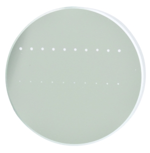
Figure 37A This photograph shows a protected aluminum-coated mirror after LIDT testing. In this particular test, it handled 0.43 J/cm2 (1064 nm, 10 ns pulse, 10 Hz, Ø1.000 mm) before damage.
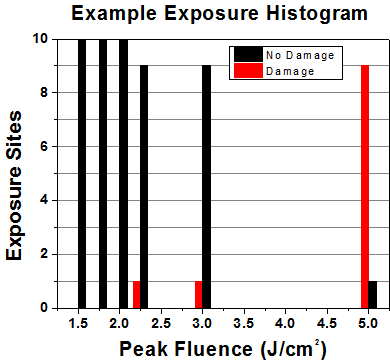
Figure 37B Example Exposure Histogram used to Determine the LIDT of
| Table 37C Example Test Data | |||
|---|---|---|---|
| Fluence | # of Tested Locations | Locations with Damage | Locations Without Damage |
| 1.50 J/cm2 | 10 | 0 | 10 |
| 1.75 J/cm2 | 10 | 0 | 10 |
| 2.00 J/cm2 | 10 | 0 | 10 |
| 2.25 J/cm2 | 10 | 1 | 9 |
| 3.00 J/cm2 | 10 | 1 | 9 |
| 5.00 J/cm2 | 10 | 9 | 1 |
According to the test, the damage threshold of the mirror was 2.00 J/cm2 (532 nm, 10 ns pulse, 10 Hz, Ø0.803 mm). Please keep in mind that these tests are performed on clean optics, as dirt and contamination can significantly lower the damage threshold of a component. While the test results are only representative of one coating run, Thorlabs specifies damage threshold values that account for coating variances.
Continuous Wave and Long-Pulse Lasers
When an optic is damaged by a continuous wave (CW) laser, it is usually due to the melting of the surface as a result of absorbing the laser's energy or damage to the optical coating (antireflection) [1]. Pulsed lasers with pulse lengths longer than 1 µs can be treated as CW lasers for LIDT discussions.
When pulse lengths are between 1 ns and 1 µs, laser-induced damage can occur either because of absorption or a dielectric breakdown (therefore, a user must check both CW and pulsed LIDT). Absorption is either due to an intrinsic property of the optic or due to surface irregularities; thus LIDT values are only valid for optics meeting or exceeding the surface quality specifications given by a manufacturer. While many optics can handle high power CW lasers, cemented (e.g., achromatic doublets) or highly absorptive (e.g., ND filters) optics tend to have lower CW damage thresholds. These lower thresholds are due to absorption or scattering in the cement or metal coating.
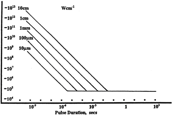
Figure 37D LIDT in linear power density vs. pulse length and spot size. For long pulses to CW, linear power density becomes a constant with spot size. This graph was obtained from [1].
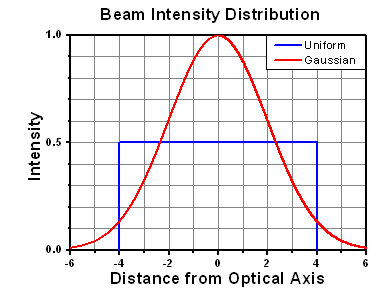
Figure 37E Intensity Distribution of Uniform and Gaussian Beam Profiles
Pulsed lasers with high pulse repetition frequencies (PRF) may behave similarly to CW beams. Unfortunately, this is highly dependent on factors such as absorption and thermal diffusivity, so there is no reliable method for determining when a high PRF laser will damage an optic due to thermal effects. For beams with a high PRF both the average and peak powers must be compared to the equivalent CW power. Additionally, for highly transparent materials, there is little to no drop in the LIDT with increasing PRF.
In order to use the specified CW damage threshold of an optic, it is necessary to know the following:
- Wavelength of your laser
- Beam diameter of your beam (1/e2)
- Approximate intensity profile of your beam (e.g., Gaussian)
- Linear power density of your beam (total power divided by 1/e2 beam diameter)
Thorlabs expresses LIDT for CW lasers as a linear power density measured in W/cm. In this regime, the LIDT given as a linear power density can be applied to any beam diameter; one does not need to compute an adjusted LIDT to adjust for changes in spot size, as demonstrated in Figure 37D. Average linear power density can be calculated using this equation.

This calculation assumes a uniform beam intensity profile. You must now consider hotspots in the beam or other non-uniform intensity profiles and roughly calculate a maximum power density. For reference, a Gaussian beam typically has a maximum power density that is twice that of the uniform beam (see Figure 37E).
Now compare the maximum power density to that which is specified as the LIDT for the optic. If the optic was tested at a wavelength other than your operating wavelength, the damage threshold must be scaled appropriately. A good rule of thumb is that the damage threshold has a linear relationship with wavelength such that as you move to shorter wavelengths, the damage threshold decreases (i.e., a LIDT of 10 W/cm at 1310 nm scales to 5 W/cm at 655 nm):

While this rule of thumb provides a general trend, it is not a quantitative analysis of LIDT vs wavelength. In CW applications, for instance, damage scales more strongly with absorption in the coating and substrate, which does not necessarily scale well with wavelength. While the above procedure provides a good rule of thumb for LIDT values, please contact Tech Support if your wavelength is different from the specified LIDT wavelength. If your power density is less than the adjusted LIDT of the optic, then the optic should work for your application.
Please note that we have a buffer built in between the specified damage thresholds online and the tests which we have done, which accommodates variation between batches. Upon request, we can provide individual test information and a testing certificate. The damage analysis will be carried out on a similar optic (customer's optic will not be damaged). Testing may result in additional costs or lead times. Contact Tech Support for more information.
Pulsed Lasers
As previously stated, pulsed lasers typically induce a different type of damage to the optic than CW lasers. Pulsed lasers often do not heat the optic enough to damage it; instead, pulsed lasers produce strong electric fields capable of inducing dielectric breakdown in the material. Unfortunately, it can be very difficult to compare the LIDT specification of an optic to your laser. There are multiple regimes in which a pulsed laser can damage an optic and this is based on the laser's pulse length. The highlighted columns in Table 37F outline the relevant pulse lengths for our specified LIDT values.
Pulses shorter than 10-9 s cannot be compared to our specified LIDT values with much reliability. In this ultra-short-pulse regime various mechanics, such as multiphoton-avalanche ionization, take over as the predominate damage mechanism [2]. In contrast, pulses between 10-7 s and 10-4 s may cause damage to an optic either because of dielectric breakdown or thermal effects. This means that both CW and pulsed damage thresholds must be compared to the laser beam to determine whether the optic is suitable for your application.
| Table 37F Laser Induced Damage Regimes | ||||
|---|---|---|---|---|
| Pulse Duration | t < 10-9 s | 10-9 < t < 10-7 s | 10-7 < t < 10-4 s | t > 10-4 s |
| Damage Mechanism | Avalanche Ionization | Dielectric Breakdown | Dielectric Breakdown or Thermal | Thermal |
| Relevant Damage Specification | No Comparison (See Above) | Pulsed | Pulsed and CW | CW |
When comparing an LIDT specified for a pulsed laser to your laser, it is essential to know the following:
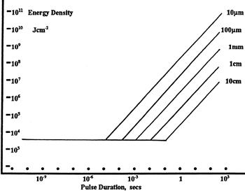
Figure 37G LIDT in energy density vs. pulse length and spot size. For short pulses, energy density becomes a constant with spot size. This graph was obtained from [1].
- Wavelength of your laser
- Energy density of your beam (total energy divided by 1/e2 area)
- Pulse length of your laser
- Pulse repetition frequency (prf) of your laser
- Beam diameter of your laser (1/e2 )
- Approximate intensity profile of your beam (e.g., Gaussian)
The energy density of your beam should be calculated in terms of J/cm2. Figure 37G shows why expressing the LIDT as an energy density provides the best metric for short pulse sources. In this regime, the LIDT given as an energy density can be applied to any beam diameter; one does not need to compute an adjusted LIDT to adjust for changes in spot size. This calculation assumes a uniform beam intensity profile. You must now adjust this energy density to account for hotspots or other nonuniform intensity profiles and roughly calculate a maximum energy density. For reference a Gaussian beam typically has a maximum energy density that is twice that of the 1/e2 beam.
Now compare the maximum energy density to that which is specified as the LIDT for the optic. If the optic was tested at a wavelength other than your operating wavelength, the damage threshold must be scaled appropriately [3]. A good rule of thumb is that the damage threshold has an inverse square root relationship with wavelength such that as you move to shorter wavelengths, the damage threshold decreases (i.e., a LIDT of 1 J/cm2 at 1064 nm scales to 0.7 J/cm2 at 532 nm):

You now have a wavelength-adjusted energy density, which you will use in the following step.
Beam diameter is also important to know when comparing damage thresholds. While the LIDT, when expressed in units of J/cm², scales independently of spot size; large beam sizes are more likely to illuminate a larger number of defects which can lead to greater variances in the LIDT [4]. For data presented here, a <1 mm beam size was used to measure the LIDT. For beams sizes greater than 5 mm, the LIDT (J/cm2) will not scale independently of beam diameter due to the larger size beam exposing more defects.
The pulse length must now be compensated for. The longer the pulse duration, the more energy the optic can handle. For pulse widths between 1 - 100 ns, an approximation is as follows:

Use this formula to calculate the Adjusted LIDT for an optic based on your pulse length. If your maximum energy density is less than this adjusted LIDT maximum energy density, then the optic should be suitable for your application. Keep in mind that this calculation is only used for pulses between 10-9 s and 10-7 s. For pulses between 10-7 s and 10-4 s, the CW LIDT must also be checked before deeming the optic appropriate for your application.
Please note that we have a buffer built in between the specified damage thresholds online and the tests which we have done, which accommodates variation between batches. Upon request, we can provide individual test information and a testing certificate. Contact Tech Support for more information.
[1] R. M. Wood, Optics and Laser Tech. 29, 517 (1998).
[2] Roger M. Wood, Laser-Induced Damage of Optical Materials (Institute of Physics Publishing, Philadelphia, PA, 2003).
[3] C. W. Carr et al., Phys. Rev. Lett. 91, 127402 (2003).
[4] N. Bloembergen, Appl. Opt. 12, 661 (1973).
In order to illustrate the process of determining whether a given laser system will damage an optic, a number of example calculations of laser induced damage threshold are given below. For assistance with performing similar calculations, we provide a spreadsheet calculator that can be downloaded by clicking the LIDT Calculator button. To use the calculator, enter the specified LIDT value of the optic under consideration and the relevant parameters of your laser system in the green boxes. The spreadsheet will then calculate a linear power density for CW and pulsed systems, as well as an energy density value for pulsed systems. These values are used to calculate adjusted, scaled LIDT values for the optics based on accepted scaling laws. This calculator assumes a Gaussian beam profile, so a correction factor must be introduced for other beam shapes (uniform, etc.). The LIDT scaling laws are determined from empirical relationships; their accuracy is not guaranteed. Remember that absorption by optics or coatings can significantly reduce LIDT in some spectral regions. These LIDT values are not valid for ultrashort pulses less than one nanosecond in duration.

Figure 71A A Gaussian beam profile has about twice the maximum intensity of a uniform beam profile.
CW Laser Example
Suppose that a CW laser system at 1319 nm produces a 0.5 W Gaussian beam that has a 1/e2 diameter of 10 mm. A naive calculation of the average linear power density of this beam would yield a value of 0.5 W/cm, given by the total power divided by the beam diameter:

However, the maximum power density of a Gaussian beam is about twice the maximum power density of a uniform beam, as shown in Figure 71A. Therefore, a more accurate determination of the maximum linear power density of the system is 1 W/cm.
An AC127-030-C achromatic doublet lens has a specified CW LIDT of 350 W/cm, as tested at 1550 nm. CW damage threshold values typically scale directly with the wavelength of the laser source, so this yields an adjusted LIDT value:

The adjusted LIDT value of 350 W/cm x (1319 nm / 1550 nm) = 298 W/cm is significantly higher than the calculated maximum linear power density of the laser system, so it would be safe to use this doublet lens for this application.
Pulsed Nanosecond Laser Example: Scaling for Different Pulse Durations
Suppose that a pulsed Nd:YAG laser system is frequency tripled to produce a 10 Hz output, consisting of 2 ns output pulses at 355 nm, each with 1 J of energy, in a Gaussian beam with a 1.9 cm beam diameter (1/e2). The average energy density of each pulse is found by dividing the pulse energy by the beam area:

As described above, the maximum energy density of a Gaussian beam is about twice the average energy density. So, the maximum energy density of this beam is ~0.7 J/cm2.
The energy density of the beam can be compared to the LIDT values of 1 J/cm2 and 3.5 J/cm2 for a BB1-E01 broadband dielectric mirror and an NB1-K08 Nd:YAG laser line mirror, respectively. Both of these LIDT values, while measured at 355 nm, were determined with a 10 ns pulsed laser at 10 Hz. Therefore, an adjustment must be applied for the shorter pulse duration of the system under consideration. As described on the previous tab, LIDT values in the nanosecond pulse regime scale with the square root of the laser pulse duration:

This adjustment factor results in LIDT values of 0.45 J/cm2 for the BB1-E01 broadband mirror and 1.6 J/cm2 for the Nd:YAG laser line mirror, which are to be compared with the 0.7 J/cm2 maximum energy density of the beam. While the broadband mirror would likely be damaged by the laser, the more specialized laser line mirror is appropriate for use with this system.
Pulsed Nanosecond Laser Example: Scaling for Different Wavelengths
Suppose that a pulsed laser system emits 10 ns pulses at 2.5 Hz, each with 100 mJ of energy at 1064 nm in a 16 mm diameter beam (1/e2) that must be attenuated with a neutral density filter. For a Gaussian output, these specifications result in a maximum energy density of 0.1 J/cm2. The damage threshold of an NDUV10A Ø25 mm, OD 1.0, reflective neutral density filter is 0.05 J/cm2 for 10 ns pulses at 355 nm, while the damage threshold of the similar NE10A absorptive filter is 10 J/cm2 for 10 ns pulses at 532 nm. As described on the previous tab, the LIDT value of an optic scales with the square root of the wavelength in the nanosecond pulse regime:

This scaling gives adjusted LIDT values of 0.08 J/cm2 for the reflective filter and 14 J/cm2 for the absorptive filter. In this case, the absorptive filter is the best choice in order to avoid optical damage.
Pulsed Microsecond Laser Example
Consider a laser system that produces 1 µs pulses, each containing 150 µJ of energy at a repetition rate of 50 kHz, resulting in a relatively high duty cycle of 5%. This system falls somewhere between the regimes of CW and pulsed laser induced damage, and could potentially damage an optic by mechanisms associated with either regime. As a result, both CW and pulsed LIDT values must be compared to the properties of the laser system to ensure safe operation.
If this relatively long-pulse laser emits a Gaussian 12.7 mm diameter beam (1/e2) at 980 nm, then the resulting output has a linear power density of 5.9 W/cm and an energy density of 1.2 x 10⁻⁴ J/cm2 per pulse. This can be compared to the LIDT values for a WPQ10E-980 polymer zero-order quarter-wave plate, which are 5 W/cm for CW radiation at 810 nm and 5 J/cm2 for a 10 ns pulse at 810 nm. As before, the CW LIDT of the optic scales linearly with the laser wavelength, resulting in an adjusted CW value of 6 W/cm at 980 nm. On the other hand, the pulsed LIDT scales with the square root of the laser wavelength and the square root of the pulse duration, resulting in an adjusted value of 55 J/cm2 for a 1 µs pulse at 980 nm. The pulsed LIDT of the optic is significantly greater than the energy density of the laser pulse, so individual pulses will not damage the wave plate. However, the large average linear power density of the laser system may cause thermal damage to the optic, much like a high-power CW beam.
Click to Enlarge
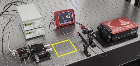
Figure 168A The beam circularization systems were placed in the area of the experimental setup highlighted by the yellow rectangle.
Comparison of Circularization Techniques for Elliptical Beams
Edge-emitting laser diodes emit elliptical beams as a consequence of the rectangular cross sections of their emission apertures. The component of the beam corresponding to the narrower dimension of the aperture has a greater divergence angle than the orthogonal beam component. As one component diverges more rapidly than the other, the beam shape is elliptical rather than circular.
Elliptical beam shapes can be undesirable, as the spot size of the focused beam is larger than if the beam were circular, and as larger spot sizes have lower irradiances (power per area). Techniques for circularizing an elliptical beam include those based on a pair of cylindrical lenses, an anamorphic prism pair, or a spatial filter. This work investigated all three approaches. The characteristics of the circularized beams were evaluated by performing M2 measurements, wavefront measurements, and measuring the transmitted power.
While it was demonstrated that each circularization technique improves the circularity of the elliptical input beam, each technique was shown to provide a different balance of circularization, beam quality, and transmitted power. The results of this work, which are documented in this Lab Fact, indicate that an application's specific requirements will determine which is the best circularization technique to choose.
Experimental Design and Setup
The experimental setup is shown in Figure 168A. The elliptically-shaped, collimated beam of a temperature-stabilized 670 nm laser diode was input to each of our circularization systems shown in Figures 168B through 168D. Collimation results in a low-divergence beam, but it does not affect the beam shape. Each system was based on one of the following:
- LJ1874L2-A and LJ1638L1-A Plano-Convex Convex Cylindrical Lenses (Figure 168B)
- PS873-A Unmounted Anamorphic Prism Pair (Figure 168C)
- Previous Generation KT310 Spatial Filter System with P5S Ø5 µm Pinhole (Figure 168D)
The beam circularization systems, shown in Figures 168B through 168D, were placed, one at a time, in the vacant spot in the setup highlighted by the yellow rectangle. With this arrangement, it was possible to use the same experimental conditions when evaluating each circularization technique, which allowed the performance of each to be directly compared with the others. This experimental constraint required the use of fixturing that was not optimally compact, as well as the use of an unmounted anamorphic prism pair, instead of a more convenient mounted and pre-aligned anamorphic prism pair.
The characteristics of the beams output by the different circularization systems were evaluated by making measurements using a power meter, a wavefront sensor, and an M2 system. In the image of the experimental setup shown in Figure 168A, all of these systems are shown on the right side of the optical table for illustrative purposes; they were used one at a time. The power meter was used to determine how much the beam circularization system attenuated the intensity of the input laser beam. The wavefront sensor provided a way to measure the aberrations of the output beam. The M2 system measurement describes the resemblance of the output beam to a Gaussian beam. Ideally, the circularization systems would not attenuate or aberrate the laser beam, and they would output a perfectly Gaussian beam.
Edge-emitting laser diodes also emit astigmatic beams, and it can be desirable to force the displaced focal points of the orthogonal beam components to overlap. Of the three circularization techniques investigated in this work, only the cylindrical lens pair can also compensate for astigmatism. The displacement between the focal spots of the orthogonal beam components were measured for each circularization technique. In the case of the cylindrical lens pair, their configuration was tuned to minimize the astigmatism in the laser beam. The astigmatism was reported as a normalized quantity.
Experimental Results
The experimental results are summarized in Table 168E, in which the green cells identify the best result in each category. Each circularization approach has its benefits. The best circularization technique for an application is determined by the system’s requirements for beam quality, transmitted optical power, and setup constraints.
Spatial filtering significantly improved the circularity and quality of the beam, but the beam had low transmitted power. The cylindrical lens pair provided a well-circularized beam and balanced circularization and beam quality with transmitted power. In addition, the cylindrical lens pair compensated for much of the beam's astigmatism. The circularity of the beam provided by the anamorphic prism pair compared well to that of the cylindrical lens pair. The beam output from the prisms had better M2 values and less wavefront error than the cylindrical lenses, but the transmitted power was lower.
| Table 168E Experimental Results | ||||||
|---|---|---|---|---|---|---|
| Method | Beam Intensity Profile | Circularitya | M2 Values | RMS Wavefront | Transmitted Power | Normalized Astigmatismb |
| Collimated Source Output (No Circularization Technique) |
 Click to Enlarge Scale in Microns |
0.36 | Y Axis: 1.63 |
0.17 | Not Applicable | 0.67 |
| Cylindrical Lens Pair |  Click to Enlarge Scale in Microns |
0.84 | X Axis: 1.90 Y Axis: 1.93 |
0.30 | 91% | 0.06 |
| Anamorphic Prism Pair |
 Click to Enlarge Scale in Microns |
0.82 | X Axis: 1.60 Y Axis: 1.46 |
0.16 | 80% | 1.25 |
| Spatial Filter |  Click to Enlarge Scale in Microns |
0.93 | X Axis: 1.05 Y Axis: 1.10 |
0.10 | 34% | 0.36 |
Components used in each circularization system were chosen to allow the same experimental setup be used for all experiments. This had the desired effect of allowing the results of all circularization techniques to be directly compared; however, optimizing the setup for a circularization technique could have improved its performance. The mounts used for the collimating lens and the anamorphic prism pair enabled easy manipulation and integration into this experimental system. It is possible that using smaller mounts would improve results by allowing the members of each pair to be more precisely positioned with respect to one another. In addition, using made-to-order cylindrical lenses with customized focal lengths may have improved the results of the cylindrical lens pair circularization system. All results may have been affected by the use of the beam profiler software algorithm to determine the beam radii used in the circularity calculation.
Additional Information
Some information describing selection and configuration procedures for several components used in this experimental work can be accessed by clicking the following hyperlinks:
| Posted Comments: | |
CHRISTIAN OLLIER
(posted 2024-07-01 05:49:06.027) Quelle est la précision sur le diamètre des trous?
Cordialement,
C.OLLIER. jdelia
(posted 2024-07-22 04:09:32.0) Thank you for reaching out. Translation: "How accurate is the diameter of the holes?" We unfortunately do not have diameter tolerances listed for these holes, however if you could provide a tolerance requirement you may have, we could look into whether this product would be suitable. I have reached out to you directly via email to discuss this further. Hyun Min Park
(posted 2022-03-28 16:31:44.94) Hello.
I want to check 2 things. Is that proper to fix pinhole to center of c mount(structure will be c mount-pinhole wheel-c mount). which kind of material are you using for pinhole.
Thank you. jdelia
(posted 2022-04-06 03:07:31.0) Thank you for contacting Thorlabs. The pinhole itself is made out of a chrome-plated fused silica substrate. We unfortunately do not have a good way to incorporate this into a C-mount system, as these are generally intended for free space applications. Atticus Russell
(posted 2020-07-17 16:43:28.97) I think the solidworks file for the P200D is broken YLohia
(posted 2020-08-24 01:37:50.0) Hello Atticus, thank you for contacting Thorlabs. I had reached out to you via email at the time of your initial feedback post, but I did not hear back from you. Could you please explain in what sense the Solidworks file is broken? I'm able to open it just fine. Does this link work for you: https://www.thorlabs.com/_sd.cfm?fileName=TTN164154-E0W.sldprt&partNumber=P200D? If it does not, please try using the STEP file: https://www.thorlabs.com/_sd.cfm?fileName=TTN164154-E0W.step&partNumber=P200D 邹 波
(posted 2020-05-28 17:57:10.377) 针孔外围的黑色氧化膜的BRDF特性是什么样的? YLohia
(posted 2020-05-28 04:27:30.0) Thank you for contacting Thorlabs. An Applications Engineer from our team in China will reach out to you directly. Kevin Sweeney
(posted 2020-02-12 14:10:55.977) How thick is the foil in the P5D? Thank you, llamb
(posted 2020-02-12 05:54:23.0) The foil from the P5D is 50 µm thick. The P5D pinhole sits inside a 40 µm deep counterbore within the foil, bringing the effective pinhole thickness down to 10 µm. user
(posted 2019-11-12 01:25:01.53) Hello. Can I purchase blank-foil-mounted disks? I want to purchase disks without a pinhole at the center.
Best regards, Sang. llamb
(posted 2019-11-13 05:26:22.0) Thank you for contacting Thorlabs. Blank mounted pinhole foils should indeed be feasible. We will reach out to you directly for this case. You may contact us at techsupport@thorlabs.com directly for any future quote requests. Sungjae Lee
(posted 2019-11-11 23:51:54.007) Which model number is possible to fit the Spatial Filter System(KT310/M)?? YLohia
(posted 2019-11-12 11:49:51.0) Hello, any of the 1" diameter lenses can be used. Please see the "Tutorial" tab on the KT310/M page for more information. Timothy Murray
(posted 2019-10-23 06:09:03.907) Unable to obtain ROHS sheet for this item YLohia
(posted 2019-10-23 08:40:57.0) Thank you for contacting Thorlabs. We will reach out to you directly with this information. Philippe Barate
(posted 2019-09-23 06:51:12.69) We need a precise position of the pinhole in a 1" tube and so for multiple pinhole. Is it possible to have the pinhole with an external thread for the mounting and always at the same position if we change the pinhole ? YLohia
(posted 2019-09-24 09:52:20.0) Hello, thank you for contacting Thorlabs. Due to the tolerances of the threads, pinhole mounting, and centration, this is not something that would be repeatable between multiple pinholes. We recommend looking into the MPH16 motorized pinhole wheel for applications that require high repeatability for pinhole switching. Jean-Baptiste Le Bouquin
(posted 2019-06-11 08:57:12.847) We just bought a P5D and cannot make light goes through the hole. When imaging the pinhole plane, one can see a ~100um structure. Could it be that some dust particule has been trapped in the pinhole ? What would be the recommended procedure ? Gently blow some air ? Thanks. llamb
(posted 2019-06-11 01:24:48.0) Thank you for contacting Thorlabs. Using a gentle burst of air is indeed recommended for clearing pinholes. However, it would be useful to see how you are imaging your pinhole. I have reached out to you directly to troubleshoot further. mathieu.guilhem
(posted 2019-02-07 16:30:21.903) Hello,
What's the thickness at aperture of the non-high-power pinholes, such as P10D and P20D ?
Thanks, llamb
(posted 2019-02-07 04:54:14.0) Thank you for your feedback. For these pinholes, the foil substrate as a whole is about 50 µm thick. The actual aperture sits inside a ~40 µm deep counterbore in the center of the foil substrate, making the effective pinhole thickness at the aperture ~10 µm. jos.grooteschaarsberg
(posted 2017-09-25 07:48:16.673) I am missing pinhole position / mount diameter tolerances for assembly of the pinhole in its mount. For exchanging the diameter, I need to know if the new pinhole in its mount is within 20 micrometer at the same centre. nbayconich
(posted 2017-10-03 05:13:38.0) Thank you for contacting Thorlabs. The positional tolerance of the pinhole is ±0.006". I will reach out to you directly. ramin.beravat
(posted 2017-04-06 17:28:23.177) Dear Sir or Madame. Can I get an annular triangle aperture? How thin can the plate be made? The thinner, the better.
Thank you very much. jlow
(posted 2017-04-17 11:27:55.0) Response from Jeremy at Thorlabs: We will contact you directly to quote this. himanaka
(posted 2016-10-26 14:13:54.867) I wonder if you have pinholes mounted on 1/2" disk? tfrisch
(posted 2016-10-31 03:16:29.0) Hello, I will contact you directly with more information on our custom capabilities. david.panak
(posted 2016-09-12 16:19:43.533) Can I get a 100 and a 200 um gold pinhole (P100C and P200C ?)
Please quote price and availability
thanks
David Panak
L-3 Greenville TX tfrisch
(posted 2016-09-15 01:32:59.0) Hello, thank you for contacting Thorlabs. I've asked our Tech Support team to prepare a quote for these custom pinholes for you. martins
(posted 2016-07-04 14:02:40.383) Hello, I purchased a pinhole P15S two months ago. After not being able to get a clean Gaussian beam, I looked at the pinhole with an electron microscope. I found that the hole is partially filled by an unknown and unwanted structure that blocks the laser beam (I can provide the corresponding images). Is there any simple way how to clean the pinhole or should I contact your Support Center to ask for replacement? Thank You. matthieu.leibovici
(posted 2016-05-06 21:09:53.357) Hi, I purchased two P10C 10um high-power precision pinholes last month. After not being able to get a clean Gaussian beam with both, I looked at the pinhole with a microscope and it looks like the diameter does not match the specs, the hole is >15um. I then imaged and tried with a P10S. The P10S pinhole looks good under microscope and I got a clean beam. Have you had a bad batch of P10C? Thanks besembeson
(posted 2016-05-10 02:56:03.0) Response from Bweh at Thorlabs USA: It is possible that you may have a unit that is out of specifications. We would also be curious to know how you determined the >15um diameter. I will contact you. tsangtimothy
(posted 2015-12-17 16:23:14.967) Am I able to purchase an unmounted one? jlow
(posted 2015-12-17 08:52:33.0) Response from Jeremy at Thorlabs: It's generally easier to use a tweezer to take out the retaining ring and get the aperture disk out. We can also provide this unmounted a special. Please contact Techsupport@thorlabs.com to inquire about the special. user
(posted 2015-12-10 10:37:33.84) Why the damage threshold is not mentioned for precision pinholes? besembeson
(posted 2015-12-10 10:32:07.0) Response from Bweh at Thorabs USA: The damage threshold guide for CW will be ~2-4 W/mm^2, 10.6um and for pulses will ~150-250KW/mm^2, 700nm, 10ns. We will be adding these values to the website subsequently. We also have a useful guide at the following link that guides you on how to adjust these values for other laser conditions: http://www.thorlabs.com/newgrouppage9.cfm?objectgroup_id=9025&tabname=Damage%20Thresholds mikhail.alekhin
(posted 2015-11-24 08:45:44.477) Hello. I want to buy a High-Power Precision Pinhole for spatial filter to convert square to Gaussian beam profile for 650 nm 1 W cw-laser.
With the threshold of 10^4 W/mm2, CW @ 10.6 µm it seems like I am on a safe side with 25 and 50 um pinholes. But I have two questions:
1) Is this threshold for "noisy" Gaussian to pure Gaussian conversion, or any-profile to Gaussian conversion. In the latter case, the pinhole, serving as a spatial filter, might absorb >50% of incident laser power.
2) 10^4 W/mm2 is measured for 10.6 µm wavelength, right? Is the threshold the same for 650 nm?
Best regards besembeson
(posted 2015-12-02 10:58:26.0) Response from Bweh at Thorlabs USA: The damage threshold is for a Gaussian beam profile. The threshold will not be the same for 650nm, which is more energetic. The value there will be reduced by a factor equivalent to the ratio of your wavelength to the specified wavelength for the damage threshold, or 0.06 (see the "Damage Threshold" tab at the following link for further details on this estimate:
http://www.thorlabs.com/newgrouppage9.cfm?objectgroup_id=3279). So the damage threshold to use for your laser is about 6 x 10^2 W/mm^2 which is lower than what you would need which means this may not be suitable for your application. michael.roth
(posted 2015-08-13 16:46:41.907) Hello,
can you tell me how much power these foils can absorb? In my application the power density is not very hight, but a large amount of the power will be absorbed (several watts).
Kind regards besembeson
(posted 2015-09-25 09:30:25.0) Response from Bweh at Thorlabs USA: The standard pinhole is made from stainless steel with a black copper oxide plating on both sides. The estimated CW damage threshold is in the order of 100kW/cm^2. We have damage threshold guides for the high power pinholes on the website. nettels
(posted 2015-02-18 17:03:56.423) To what precision are the pinholes centered in the 1' mount?
Thank you.
Daniel cdaly
(posted 2015-02-24 04:57:06.0) Response from Chris at Thorlabs: While the tolerances on the centration of the mount and the internal foil are quite good, the foil sits in the mount somewhat loosely, so the overall centration is really not well defined. If a well tolerances position on the pinhole is needed, we can have the foil epoxied into the mount before cutting as a custom. Any requests for these items should come to us at techsupport@thorlabs.com. carlos.macias
(posted 2015-01-26 11:42:19.607) We bought a few of your high power pinholes (P50C) to build a spatial filter for our femtosecond laser (150 fs, 1030 nm). The quoted threshold for a 10 ns pulse @ 700 nm is 100 MW/cm2. We are focusing our laser to a spot diameter of 65 µm with 1 W of power. So we have an irradiance of ~0.04 MW/cm2. To take into account the difference in pulse durations and wavelength, we use a factor of ~200. Then the supposed damage threshold of the pinhole should be around 0.5 MW/cm2. This is still one order of magnitude larger than our irradiance. So the pinholes worked fine for a couple of days and after the second day, they were all destroyed. We made sure that the pinholes were aligned correctly using low powers (50 mW), before increasing te power to 1 W. Could you then explain why all of the four pinholes we bought did not support the irradiance after two days? Heat slowly destroyed the gold plating? Would it be possible to produce pinholes that would work for us? cdaly
(posted 2015-01-29 09:09:37.0) Response from Chris at Thorlabs: I'm afraid we do not have a spec for the damage threshold of the pinhole for femto-second pulses. Pulses shorter than 10^-9 s cannot be compared to our specified LIDT values with much reliability. In this ultra-short-pulse regime various mechanics, such as multiphoton-avalanche ionization, take over as the predominate damage mechanism. In contrast, pulses between 10^-7 s and 10^-4 s may cause damage to an optic either because of dielectric breakdown or thermal effects. bruno.tremblay
(posted 2015-01-08 12:27:37.747) I experience problem with my two 5µm pinhole.
I notice that after 5 years, light intensity ratio going through a 10µm pinhole relative to 25µm pinhole stayed the same.
But for a 5 µm pinhole relative to the 10µm pinhole, the ratio change by -30% in one case and -50% for the second one.
Is there some long term stability issue which could make that situation normal for small pinhole?
Regards
Bruno cdaly
(posted 2015-01-20 03:34:27.0) Response from Chris at Thorlabs: This is not something we have ever seen before, but we will contact you directly to discuss this further. araf
(posted 2014-03-27 11:04:34.9) Hi,
Could these be made with half inch outermost diameters (SM05/16mm cage compatible)? I'm wishing to perform spatial filtering, but I want to have things as compact as possible. I would also like to utilize the shorter focal length half-inch lenses.
Thanks! jlow
(posted 2014-03-27 11:24:25.0) Response from Jeremy at Thorlabs: We can provide these pinholes in Ø1/2" package as a custom. We will contact you directly for the quote. scienc2
(posted 2014-03-18 14:17:46.877) Hello,
Can you customize a pinhole product that have two pinholes with different sizes on one pinhole product? Also, can you provide the pinhole product without any housing?
Thank you.
Best regards,
Kim, Juwan jlow
(posted 2014-03-18 08:59:38.0) Response from Jeremy at Thorlabs: We can do custom pinholes. We will contact you directly about this. makarov
(posted 2014-02-03 20:51:22.433) Can you estimate damage threshold for CW light (at 808 nm or at 700 nm) for standard non-high-power pinhole? jlow
(posted 2014-02-04 03:08:09.0) Response from Jeremy at Thorlabs: The standard pinhole is made from stainless steel with a black copper oxide plating on both sides. The estimated CW damage threshold is on the order of 100kW/cm^2. l.gerencser
(posted 2013-05-06 12:54:59.367) Could you provide me any information about the damage threshold of the standard (non high power) variant of the precision pinholes for the following laser parameters?
700 nm, 140 fs pulse width, 80 Mhz repetition rate jlow
(posted 2013-05-09 15:49:00.0) Response from Jeremy at Thorlabs: We do not have a spec for the damage threshold of the pinhole for femto-second pulses. For a 10ns pulse at 700nm, the damage threshold is estimated to be around 150kW/mm^2. ihyun2010
(posted 2013-04-15 00:22:30.093) I want to make pinhole like P20S with 3 lows and 3 columns. How can I contact you for this item? tcohen
(posted 2013-04-18 15:19:00.0) Response from Tim at Thorlabs: Thank you for your inquiry. We can assist with customs through our technical support department at techsupport@thorlabs.com. I will contact you directly to discuss this. tcohen
(posted 2012-10-04 13:23:00.0) Response from Tim at Thorlabs: The damage thresholds for the high-power C series are specified with the gold plated side incident. The standard S series are on the order of 100kW/mm^2 for 10ns, 700nm. user
(posted 2012-10-03 13:35:09.0) What is the damage threshold of the mounted pinholes (S-series)? As for the high-power (C-series) ones, which side is facing the laser beam (the catalog page is slightly controversial)? bdada
(posted 2011-09-22 20:32:00.0) Response from Buki at Thorlabs:
We do not have exactly what you are looking for but we have submitted your request to our design team. In the meantime, please consider if our zero aperture iris, SM1D12SZ, may be suitable for your application. We also have variable iris diaphraphms:
http://www.thorlabs.com/NewGroupPage9.cfm?ObjectGroup_ID=1479
http://www.thorlabs.com/NewGroupPage9.cfm?ObjectGroup_ID=220 akde
(posted 2011-09-13 00:44:03.0) I used the cage system to construct a fluorescence microscope for single-molecule detection. I found the parasitic light is a source of huge noise in the system. The cage components may be colored black to prevent this. Better light isolation may be achieved by using a tube system where all optics (lenses, apertures etc) may be mounted inside a tube to result in robust alignment as well. Presently I am using a combination of cages and tubes.
Dr Arijit K De (Postdoc, LBNL/UCBerkeley) akde
(posted 2011-09-13 00:36:41.0) For few specific applications, e.g. spatial filtering in confocal fluorescence detection etc, larger apertures (>150um) are often needed as a smaller pinhole reduces the signal level in addition to background rejection. A series of such apertures with varying sizes (200um, 500um & 1mm) on a 1" sm1 mount will be of great interest. jjurado
(posted 2011-07-22 10:30:00.0) Response from Javier at Thorlabs to valeri.abrahamyan: Thank you very much for your interest in our products. To purchase our products, you can contact us at sales@thorlabs.com or by phone at (973) 579 7227. You can also create an account with us online and purchase our products through the web. You can create your own account here:
http://www.thorlabs.com/login.cfm?lc=create
I will contact you directly for further assistance. valeri.abrahamyan
(posted 2011-07-21 17:13:08.0) I wont to purchase your praducts jjurado
(posted 2011-07-19 18:16:00.0) Response from Javier at Thorlabs to cmansfield: Thank you very much for contacting us. We can certainly offer a 200 um mounted pinhole. I will contact you directly with a quotation. cmansfield
(posted 2011-07-19 12:32:04.0) Do you have a 200 um mounted pinhole?
Can you make one if not?
I would rather not buy the 3/8" Diameter pinhole from Edmund. Thorlabs
(posted 2010-10-27 17:00:59.0) Response from Javier at Thorlabs to Ron Palfenier: the outer diameter of the unmounted pinhole is 0.375" (9.53mm). ron.palfenier
(posted 2010-10-27 12:02:50.0) If the pinhole were removed from the 1 inch holder, what would be the O.D. size of the un-mounted pinhole? klee
(posted 2009-09-08 12:04:21.0) A response from Ken at Thorlabs to wwarger: We can make 1/2" mounted pinholes as specials. Please send an email to techsupport@thorlabs.com, with the size and quantity that you need, and we will send you a quotation. wwarger
(posted 2009-09-03 14:13:47.0) You should consider making 1/2" mounted pinholes to fit in the SM05 mounts and 16 mm cage plates. Laurie
(posted 2008-05-27 09:31:50.0) Response from Laurie at Thorlabs to cm1105: The mounted pinholes are fabricated from 302 nonmagnetic stainless steel. If you have additional questions, please dont hesitate to ask. cm1105
(posted 2008-05-27 08:41:52.0) of which material are the pinholes made? Laurie
(posted 2008-03-18 12:50:14.0) Response from Laurie at Thorlabs to cm1105: The specified dimension in the price box is the diameter of the pinhole. This certainly isnt clear, so we will change the item description to prevent future confusion. cm1105
(posted 2008-03-18 12:37:38.0) The specified dimension is the radius or the diameter of the pinhole? acable
(posted 2007-10-17 14:50:18.0) Is the CW power rating measured at 10.6um or 1.06um. techsupport
(posted 2007-10-17 11:25:37.0) add a definition of the parameter circularity which is mentioned on the overview tab |
| Apertures Selection Guide | |||
|---|---|---|---|
| Aperture Type | Representative Image (Click to Enlarge) |
Description | Aperture Sizes Available from Stocka |
| Single Precision Pinholesa |
 |
Circular Pinholes in Stainless Steel Foils | Ø1 µm to Ø9 mm |
 |
Circular Pinholes in Stainless Steel Foils, Vacuum Compatible |
Ø5 µm to Ø2 mm | |
 |
Circular Pinholes in Gold-Plated Copper Foils | Ø5 µm to Ø2 mm | |
 |
Circular Pinholes in Gold-Plated Copper Foils with High-Power Housings |
Ø5 µm to Ø500 µm | |
 |
Circular Pinholes in Tungsten Foils | Ø5 µm to Ø2 mm | |
 |
Circular Pinholes in Molybdenum Foils | Ø5 µm to Ø2 mm | |
 |
Square Pinholes in Stainless Steel Foils | 100 to 1000 µm Square | |
| Slitsa |  |
Slits in Stainless Steel Foils | 3 mm Slit Lengths: 5 to 500 µm Widths 10 mm Slit Lengths: 20 to 500 µm Widths |
 |
Double Slits in Stainless Steel Foils | 3 mm Slit Lengths with 40, 50, or 100 µm Widths, Spacing of 3X or 6X the Slit Width |
|
| Half-Apertures |  |
Mounted, Half-Aperture Foils | Half-Apertures for Knife-Edge Scan Measurements |
| Annular Apertures |  |
Annular Aperture Obstruction Targets on Quartz Substrates with Chrome Masks |
Ø1 mm Apertures with ε Ratiosb from 0.05 to 0.85 Ø2 mm Aperture with ε Ratiob of 0.85 |
| Pinhole Wheels |  |
Manual, Mounted, Chrome-Plated Glass Disks with Lithographically Etched Pinholes |
Each Disk has 16 Pinholes from Ø25 µm to Ø2 mm and Four Annular Apertures (Ø100 µm Hole, 50 µm Obstruction) |
 |
Motorized Pinhole Wheels with Chrome-Plated Glass Disks with Lithographically Etched Pinholes |
Each Disk has 16 Pinholes from Ø25 µm to Ø2 mm and Four Annular Apertures (Ø100 µm Hole, 50 µm Obstruction) |
|
| Pinhole Kits |  |
Stainless Steel Precision Pinhole Kits | Kits of Ten Circular Pinholes in Stainless Steel Foils Covering Ø5 µm to Ø9 mm |
 Products Home



 Pinhole Wheels