 产品首页
产品首页半波液晶可变延迟器/波片
- Nematic Liquid Crystal Half-Wave Variable Retarders
- Available with Ø10 mm or Ø20 mm Clear Aperture
- AR Coated for Visible, NIR, or MIR Light
- Compensated Models Achieve 0 nm Retardance
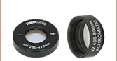
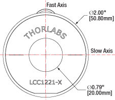
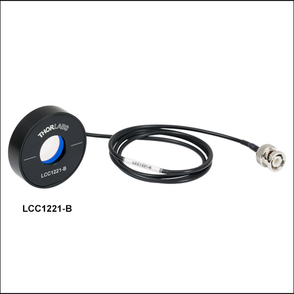
LCC1221-B
Ø20 mm Clear Aperture,
<20 ms Switching Time,
Mounted, Uncompensated
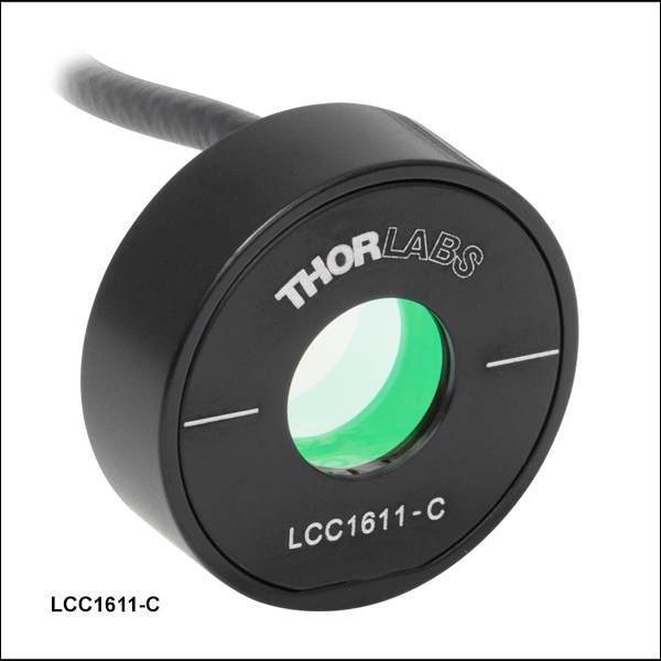
LCC1611-C
Ø10 mm Clear Aperture,
<23 ms Switching Time,
Mounted, Compensated
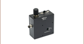
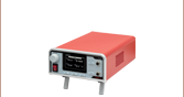
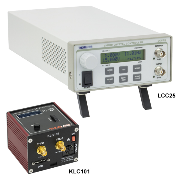
LCC25
Benchtop LC Controller
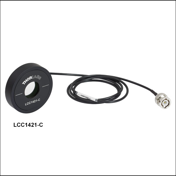
LCC1421-A
Ø20 mm Clear Aperture,
<17 ms Switching Time,
Mounted, Compensated
KLC101
K-Cube® LC Controller
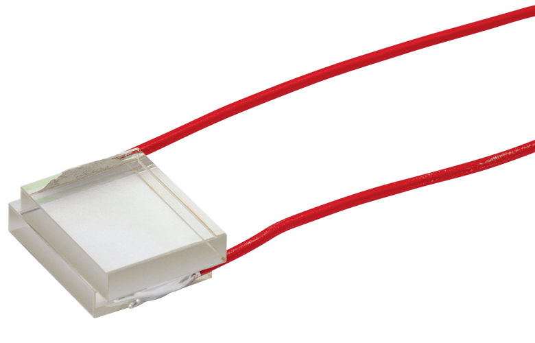
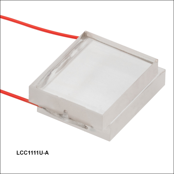
LCC1111U-A
Ø10 mm Clear Aperture,
<10 ms Switching Time,
Unmounted, Uncompensated


Please Wait
工作原理
高延迟
低延迟
图 1:向列相液晶分子有序排列,分子呈现拉伸状,具有光学各向异性。施加电场时,分子沿电场排列,双折射的水平由液晶分子的倾斜控制。
残余延迟量补偿
Click to Enlarge
无补偿的LC延迟器
Click to Enlarge
有补偿的LC延迟器
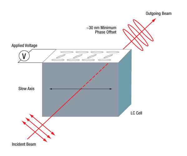
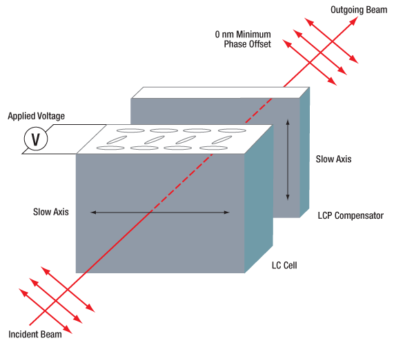
图 2:无补偿的液晶延迟器的最小延迟量为~30 nm。我们有补偿的LC延迟器包含具有固定延迟和慢轴的液晶聚合物补偿器,慢轴与可变液晶盒的慢轴垂直。这样,我们有补偿的延迟器就可以实现0 nm的最小延迟。
| Selection Guide for LC Retarders | |
|---|---|
| Type | Clear Aperture |
| Half Wave | Ø10 mm or Ø20 mm |
| Half Wave, Thermally Stabilized | Ø10 mm |
| Full Wave | Ø10 mm or Ø20 mm |
| Full Wave, Thermally Stabilized | Ø20 mm |
| Multi-Wave | Ø10 mm |
| Multi-Wave, Integrated Controller | Ø10 mm |
| Custom LC Retarders | |
特性
- 可变波片主动控制光的偏振态和/或相位延迟
- 延迟范围:
- 0 nm到λ/2,用于带残余延迟量补偿的LC延迟器
- ~30 nm到λ/2,用于无补偿的LC延迟器
- 通光孔径:Ø10 mm或Ø20 mm
- Ø10 mm孔径的版本有已安装和未安装型号可选
- 快速响应的Ø10 mm延迟器在25 °C时上升+下降时间低至~3.0 ms
- 整个通光孔径上的延迟均匀度高(详情请看规格标签)
- 兼容我们的LCC25和KLC101电压控制器(单独出售)
Thorlabs的半波液晶可变延迟器(LCVR)将向列相液晶盒用作可变波片。由于没有移动部件,可实现毫秒级的快速响应时间(详情请看响应时间标签)。我们提供五种常用波长范围的增透膜:350 - 700 nm、650 - 1050 nm、1050 - 1700 nm、1650 - 3000 nm或3600 - 5600 nm(透过率和延迟量数据,请看性能标签)。
Thorlabs提供两种通光孔径的尺寸:Ø10 mm和Ø20 mm。两种尺寸都有两种可变延迟范围可选:0 nm到λ/2的延迟,用于带残余延迟量补偿的延迟器;~30 nm到λ/2的延迟,用于无补偿的LC延迟器。我们有补偿的延迟器集成了由液晶聚合物制成的相位补偿器,可以补偿LCVR的残余延迟量,以在特定的驱动电压下达到真实零延迟量(更多信息,请看性能标签)。有关结构与原理,请看下方所述。
Ø10 mm延迟器的外径为1英寸,兼容我们的Ø1英寸光学元件安装座。此外,我们还有一款通光孔径Ø10 mm的未安装版特殊延迟器,即LCC1111U-A,这种结构紧凑的LCVR适合OEM和其他特殊应用。Ø20 mm延迟器的外径为2英寸,兼容我们的Ø2英寸光学元件安装座。有关推荐的兼容安装座,请看规格标签。
性能
这些液晶可变延迟器均匀度良好,光损耗低且波前畸变小。此外,它们响应迅速,工作温度范围广,波长范围广。详情请见规格、性能和响应时间标签。我们同样提供热稳定半波延迟器,具有更好的长期稳定性能。
快速响应的Ø10 mm延迟器
Ø10 mm通光孔径的LCC1511-x无补偿和LCC1611-x有补偿LCVR采用不同的向列相液晶材料,响应速度比LCC1111-D、LCC1111-MIR和Ø20 mm LCVR提高了超过3倍。
上一代Ø10 mm延迟器
如果您的应用不需要LCC1511-x和LCC1611-x LCVR的快速响应,可以联系技术支持techsupport-cn@thorlabs.com获取上一代Ø10 mm通光孔径的延迟器,它们与Ø20 mm LCVR的规格相同,使用的也是相同的向列相液晶材料。详情请看定制能力标签。
工作
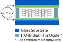
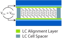
如图 1所示,液晶可变延迟器由填满液晶(LC)分子溶液的透明液晶盒构成,用作可变波片。在未加电压的情况下,LC分子的取向由取向膜决定。取向膜由有机聚酰亚胺(PI)膜层构成,分子在制造期间沿摩擦方向排列。由于LC材料的双折射性,LC延迟器可以用作光学各向异性波片,机械外壳上标有慢轴,与延迟器的表面平行。液晶盒壁的两个平行面镀有透明导电膜,可在液晶盒上施加电压。施加交流电压后,LC分子会根据所施电压Vrms改变默认排列方向。因此,改变施加电压可以主动控制液晶可变延迟器的延迟。
残余延迟量补偿
由于PI层表面锚定,即使施加电压,仍有一些液晶分子无法改变方向,尤其是靠近取向膜层的分子。这样,LC延迟器在工作期间产生了残余延迟量。Thorlabs无补偿的LC延迟器在25 Vrms驱动电压下具有~30 nm的残余延迟量,如上面的图 2所示。为了满足敏感应用中真实零延迟量的需要,我们提供有补偿的LC延迟器。由液晶聚合物(LCP)构成的补偿层粘在液晶盒上,慢轴垂直于液晶盒的慢轴。LCP补偿层的固定延迟量为~50 nm。因此,特定驱动电压在5 V到20 V之间时,液晶盒与补偿器的延迟量相互抵消,产生真实零延迟量。但是,这样可能导致延迟均匀度稍微变低,总厚度增加。更多信息,请看规格和性能标签。
控制器
虽然采用交流电压(0到25 Vrms),但LCC25和KLC101控制器提供主动直流偏移补偿。直流偏移补偿自动将液晶设备的直流偏压置零,以抵消电荷积累。
有补偿的半波液晶延迟器
| Item # | LCC1611-A | LCC1421-A | LCC1611-B | LCC1421-B | LCC1611-C | LCC1421-C | |
|---|---|---|---|---|---|---|---|
| Wavelength Range | 350 - 700 nma | 650 - 1050 nm | 1050 - 1700 nm | ||||
| Retardance Rangeb | 0 nm to >λ/2 | ||||||
| Clear Aperture | Ø10 mm | Ø20 mm | Ø10 mm | Ø20 mm | Ø10 mm | Ø20 mm | |
| Housing Outer Dimensions | Ø1"c (Ø25.4 mm) | Ø2.20"d (Ø55.8 mm) | Ø1"c (Ø25.4 mm) | Ø2.20"d (Ø55.8 mm) | Ø1"c (Ø25.4 mm) | Ø2.20"d (Ø55.8 mm) | |
| Liquid Crystal Material | Nematic Liquid Crystal | ||||||
| Surface Quality | 60-40 Scratch-Dig | ||||||
| Parallelism | < 5 arcmin | ||||||
| Switching Time (Rise/Fall, Typical)e | 3.34 ms / 0.14 ms @ 25 °C, 635 nm | 15.8 ms / 260 µs @ 22 °C, 635 nm | 4.01 ms / 0.27 ms @ 25 °C, 780 nm | 34.0 ms / 360 µs @ 22 °C, 780 nm | 22.34 ms / 0.55 ms @ 25 °C, 1550 nm | 152 ms / 510 µs @ 25.6 °C, 1550 nm | |
| Operating Voltage (Max)f | 25 V | ||||||
| Damage Threshold | Pulsed (ns) | 1.0 J/cm2 (532 nm, 10 Hz, 8 ns, Ø200 µm) | 1.7 J/cm2 (810 nm, 10 Hz, 7.6 ns, Ø234 µm) | 1.2 J/cm2 (1542 nm, 10 Hz, 10 ns, Ø458 µm) | |||
| Pulsed (fs) | 0.01 J/cm2 (532 nm, 100 Hz, 76 fs, Ø162 µm) | 0.01 J/cm2 (800 nm, 100 Hz, 36.4 fs, Ø189 µm) | 0.08 J/cm2 (1550 nm, 100 Hz, 70 fs, Ø145 µm) | ||||
| AR Coatingg | Ravg < 0.5% | ||||||
| Wavefront Distortion | ≤λ/4 @ 635 nm | ||||||
| Retardance Uniformity (RMS)h | < λ/20 @ 400 nm | < λ/20 @ 650 nm | < λ/20 @ 1050 nm | ||||
| Housing Thickness | 8.6 mm (0.34") | 15.0 mm (0.59") | 8.6 mm (0.34") | 15.0 mm (0.59") | 8.6 mm (0.34") | 15.0 mm (0.59") | |
| Storage Temperature | -30 to 70 °C | ||||||
| Operation Temperature | -20 to 45 °C | ||||||
无补偿的半波液晶延迟器
| Item # | LCC1111U-A | LCC1511-A | LCC1221-A | LCC1111U-B | LCC1511-B | LCC1221-B | |
|---|---|---|---|---|---|---|---|
| Wavelength Range | 350 - 700 nma | 650 - 1050 nm | |||||
| Retardance Rangeb | ~30 nm to >λ/2 | ||||||
| Clear Aperture | Ø10 mm | Ø10 mm | Ø20 mm | Ø10 mm | Ø10 mm | Ø20 mm | |
| Housing Outer Dimensions | 17.0 mm × 12.0 mm (0.67" × 0.47") | Ø1"c (Ø25.4 mm) | Ø2"d (Ø50.8 mm) | 17.0 mm x 12.0 mm (0.67" x 0.47") | Ø1"c (Ø25.4 mm) | Ø2"d (Ø50.8 mm) | |
| Liquid Crystal Material | Nematic Liquid Crystal | ||||||
| Surface Quality | 40-20 Scratch-Dig | ||||||
| Parallelism | < 5 arcmin | ||||||
| Switching Time (Rise/Fall, Typical)e | 9.8 ms / 0.24 ms @ 25 °C, 635 nm | 2.72 ms / 0.16 ms @ 25 °C, 635 nm | 9.8 ms / 0.24 ms @ 25 °C, 635 nm | 19.52 ms / 0.44 ms @ 25 °C, 780 nm | 3.41 ms / 0.24 ms @ 25 °C, 780 nm | 19.52 ms / 0.44 ms @ 25 °C, 780 nm | |
| Operating Voltage (Max)f | 25 V | ||||||
| Damage Threshold | Pulsed (ns) | 1.0 J/cm2 (532 nm, 10 Hz, 8 ns, Ø200 µm) | 1.7 J/cm2 (810 nm, 10 Hz, 7.6 ns, Ø234 µm) | ||||
| Pulsed (fs) | 0.01 J/cm2 (532 nm, 100 Hz, 76 fs, Ø162 µm) | 0.01 J/cm2 (800 nm, 100 Hz, 36.4 fs, Ø189 µm) | |||||
| AR Coatingg | Ravg < 0.5% | ||||||
| Wavefront Distortion | ≤λ/4 @ 635 nm | ||||||
| Retardance Uniformity (RMS)h | < λ/50 @ 400 nm | < λ/50 @ 650 nm |
|||||
| Housing Dimensional Tolerance | ±0.4 mm | - | ±0.4 mm | - | |||
| Housing Thickness | 6.0 mm (0.24") | 8.0 mm (0.32") | 13.0 mm (0.51") | 6.0 mm (0.24") | 8.0 mm (0.32") | 13.0 mm (0.51") | |
| Storage Temperature | -30 to 70 °C | ||||||
| Operation Temperature | -20 to 45 °C | ||||||
| Item # | LCC1511-C | LCC1221-C | LCC1111-D | LCC1111-MIR | |
|---|---|---|---|---|---|
| Wavelength Range | 1050 - 1700 nm | 1650 - 3000 nm | 3600 - 5600 nm | ||
| Retardance Rangea | ~30 nm to >λ/2 | ~30 nm to >λ/2 | ~30 nm to >λ/2 | ~30 nm to >λ/2 | |
| Clear Aperture | Ø10 mm | Ø20 mm | Ø10 mm | Ø10 mm | |
| Housing Outer Dimensions | Ø1"b (Ø25.4 mm) | Ø2"c (Ø50.8 mm) | Ø1"b (Ø25.4 mm) | Ø1"b (Ø25.4 mm) | |
| Liquid Crystal Material | Nematic Liquid Crystal | ||||
| Surface Quality | 40-20 Scratch-Dig | 60-40 Scratch-Dig | |||
| Parallelism | < 5 arcmin | ||||
| Switching Time (Rise/Fall, Typical)d | 21.29 ms / 0.50 ms @ 25 °C, 1550 nm | 95.8 ms / 1.81 ms @ 25.6 °C, 1550 nm | 192 ms / 1 ms @ 25.6 °C, 2200 nm | 372 ms / 14 ms @ 25.6 °C, 4400 nm | |
| Operating Voltage (Max)e | 25 V | ||||
| Damage Threshold | Pulsed (ns) | 1.2 J/cm2 (1542 nm, 10 Hz, 10 ns, Ø458 µm) | 0.041 J/cm2 (2000 nm, 10 Hz, 6.5 ns, Ø292 µm) | N/A | |
| Pulsed (fs) | 0.08 J/cm2 (1550 nm, 100 Hz, 70 fs, Ø145 µm) | 0.025 J/cm2 (2000 nm, 100 Hz, 100 fs, Ø220 µm) | N/A | ||
| AR Coatingf | Ravg < 0.5% | Ravg < 1.0% | |||
| Wavefront Distortion | ≤λ/4 @ 635 nm | - | |||
| Retardance Uniformity (RMS)g | < λ/50 @ 1050 nm | < λ/30 @ 1650 nm | < λ/10 @ 3600 nm | ||
| Housing Thickness | 8.0 mm (0.32") | 13.0 mm (0.51") | 8.0 mm (0.32") | 8.0 mm (0.32") | |
| Storage Temperature | -30 to 70 °C | ||||
| Operation Temperature | -20 to 45 °C | ||||
| Variable Half-Wave Retarder Performance Graphs | |||||
|---|---|---|---|---|---|
| Item #a | Wavelength Range | Retardance @ 25 °C | Retardance vs. Temperature | Temperature Stability | Transmission |
| LCC1611-A | 350 - 700 nm | 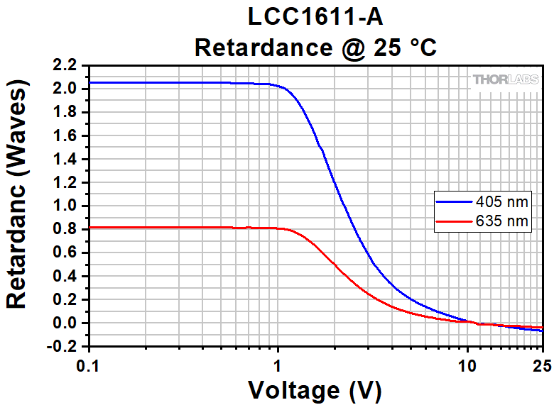 | 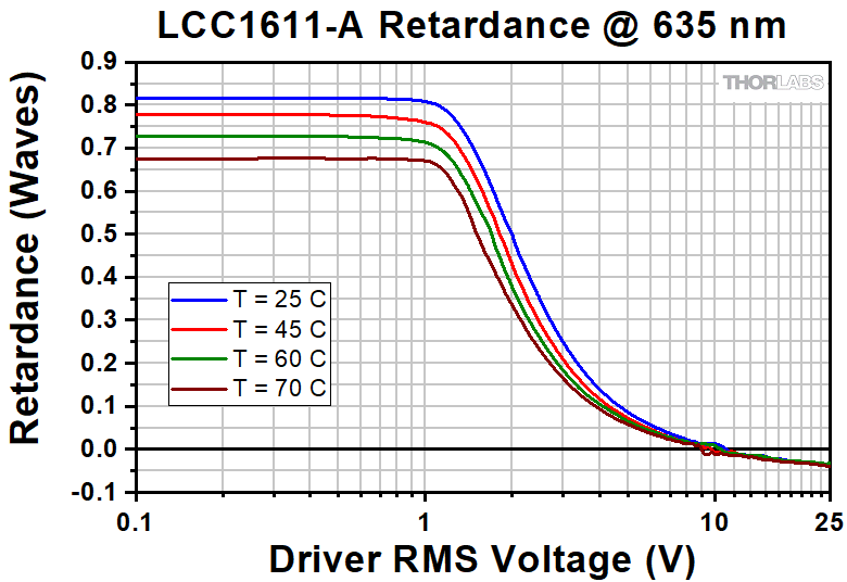 (635 nm) (635 nm) | 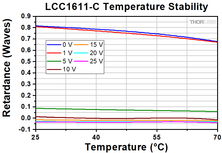 | |
| LCC1511-A | 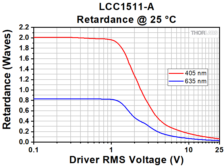 | 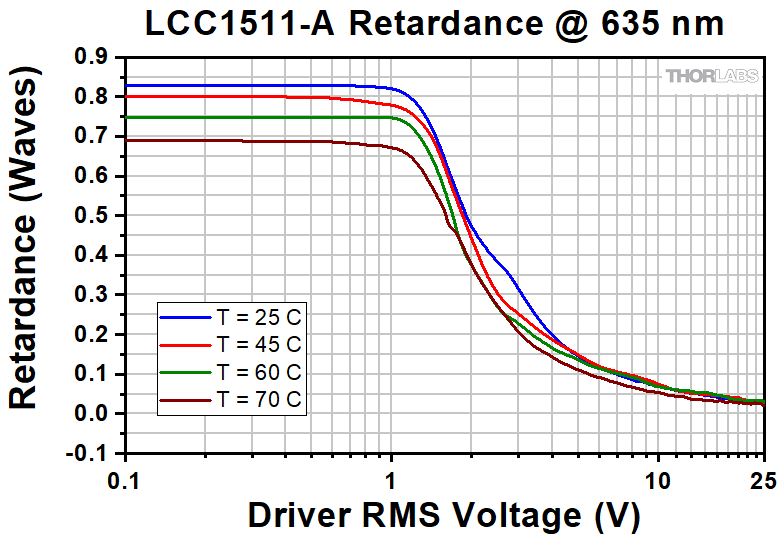 (635 nm) (635 nm) | 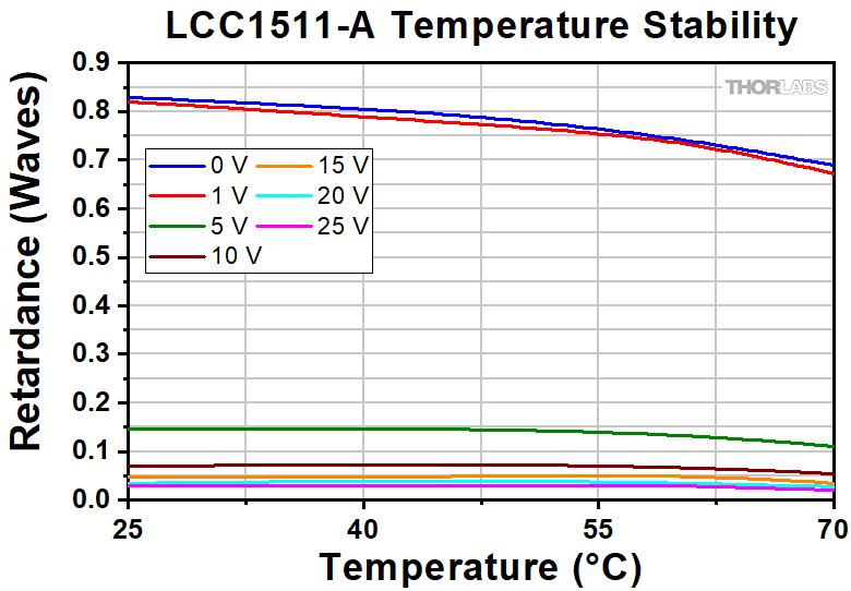 | ||
| LCC1421-A |  | 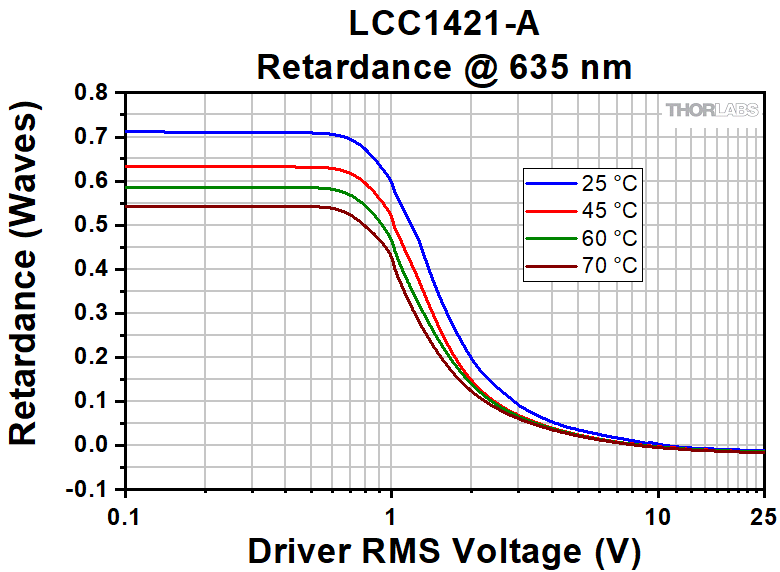 (635 nm) (635 nm) | 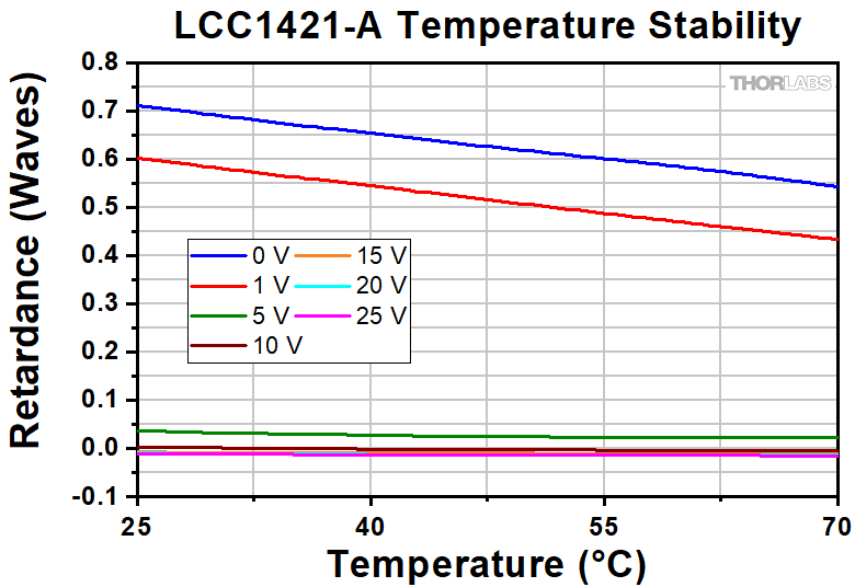 | ||
| LCC1221-A, LCC1111U-A | 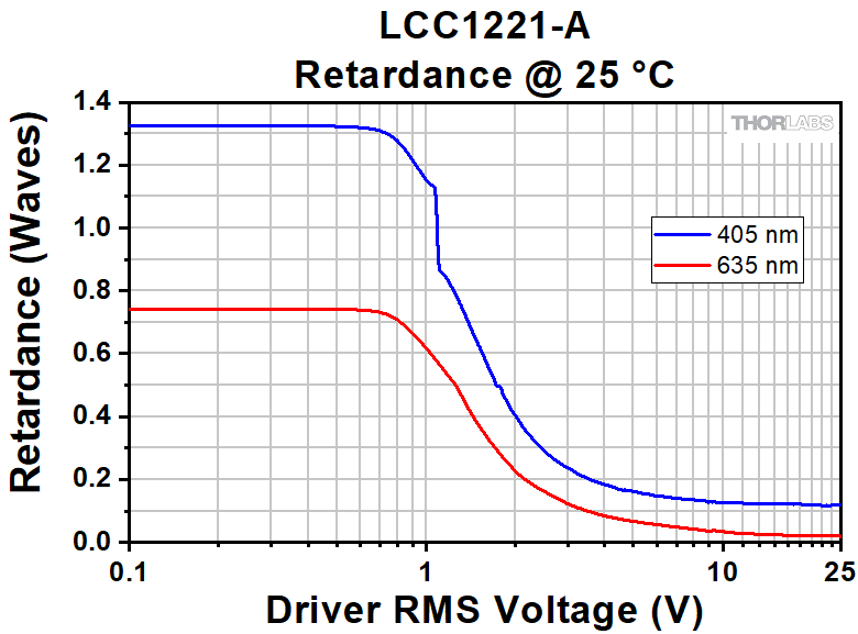 | 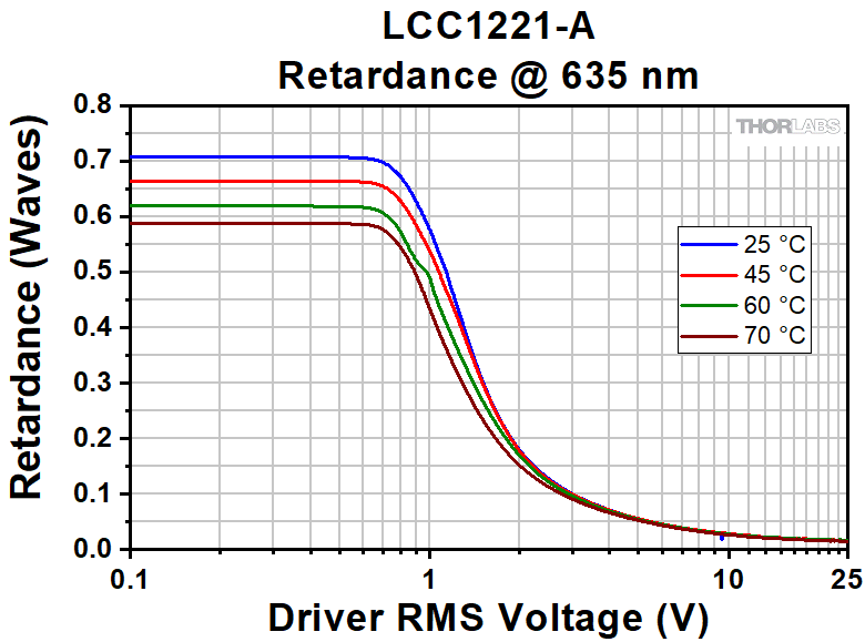 (635 nm) (635 nm) | 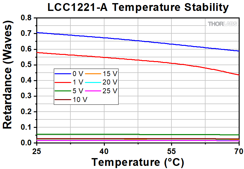 | ||
| LCC1611-B | 650 - 1050 nm | 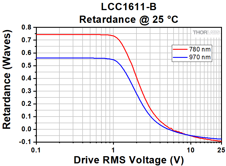 |  (780 nm) (780 nm) | 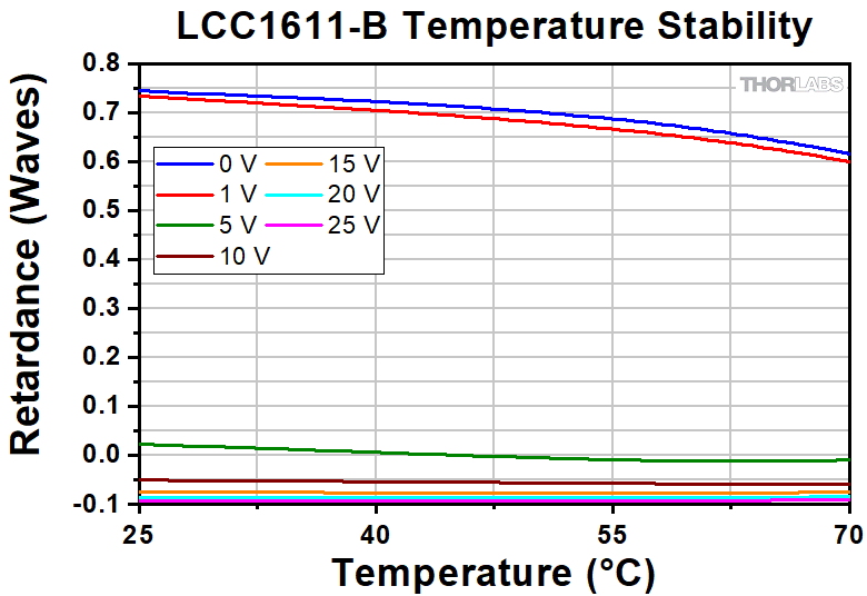 | |
| LCC1511-B |  |  (780 nm) (780 nm) |  | ||
| LCC1421-B |  | 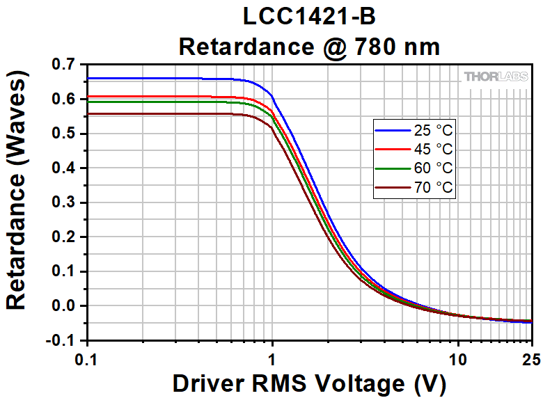 (780 nm) (780 nm) | 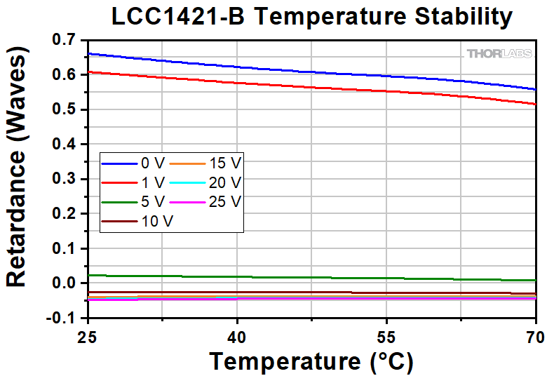 | ||
| LCC1221-B, LCC1111U-B | 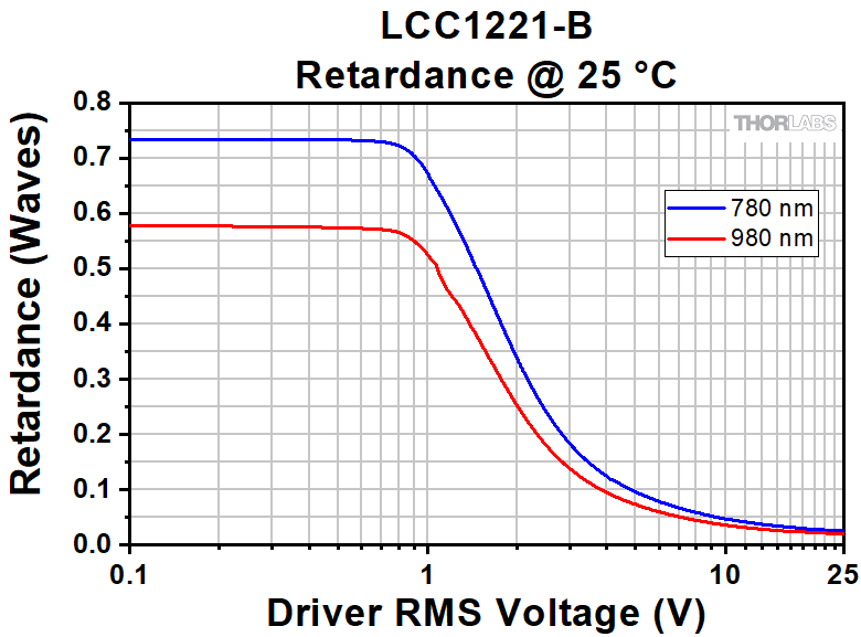 | 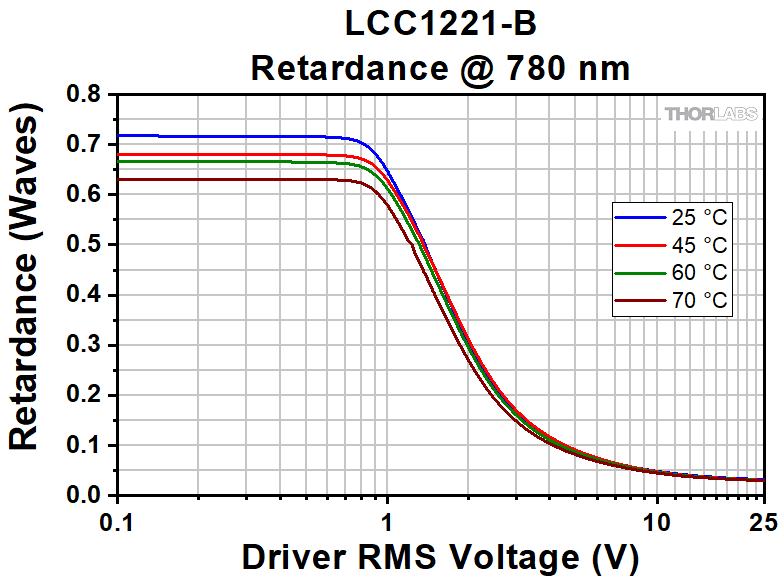 (780 nm) (780 nm) |  | ||
| LCC1611-C | 1050 - 1700 nm |  |  (1550 nm) (1550 nm) |  | |
| LCC1511-C |  | 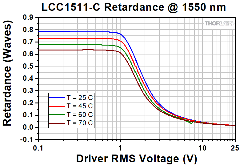 (1550 nm) (1550 nm) | 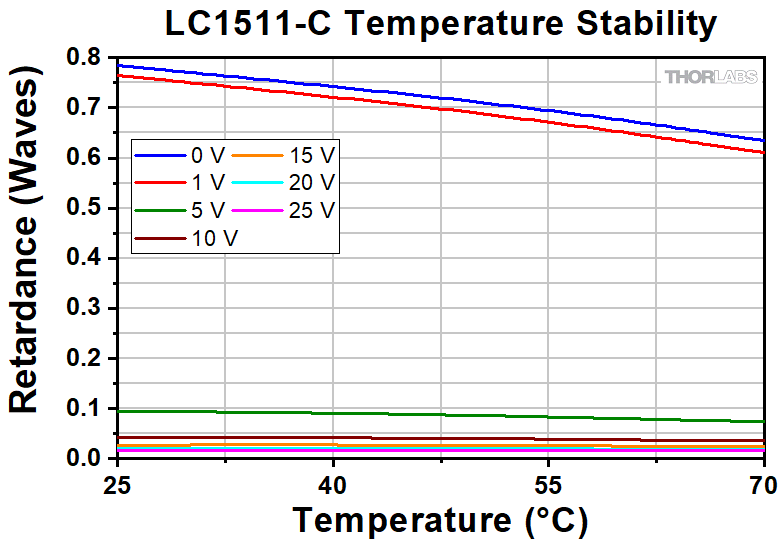 | ||
| LCC1421-C | 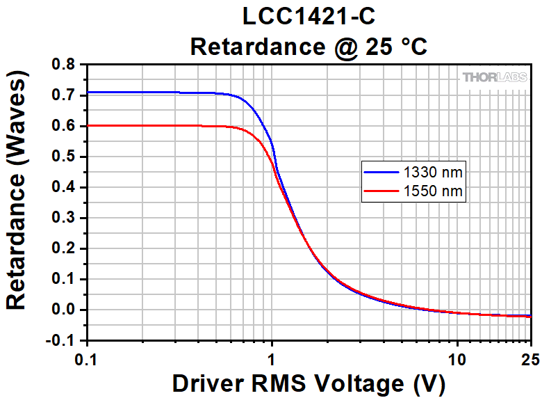 | 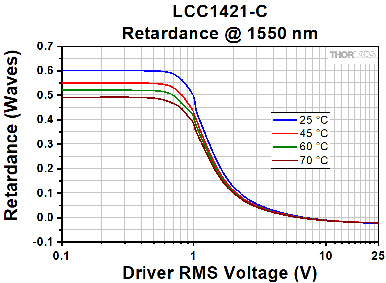 (1550 nm) (1550 nm) |  | ||
| LCC1221-C |  |  (1550 nm) (1550 nm) |  | ||
| LCC1111-D | 1650 - 3000 nm | 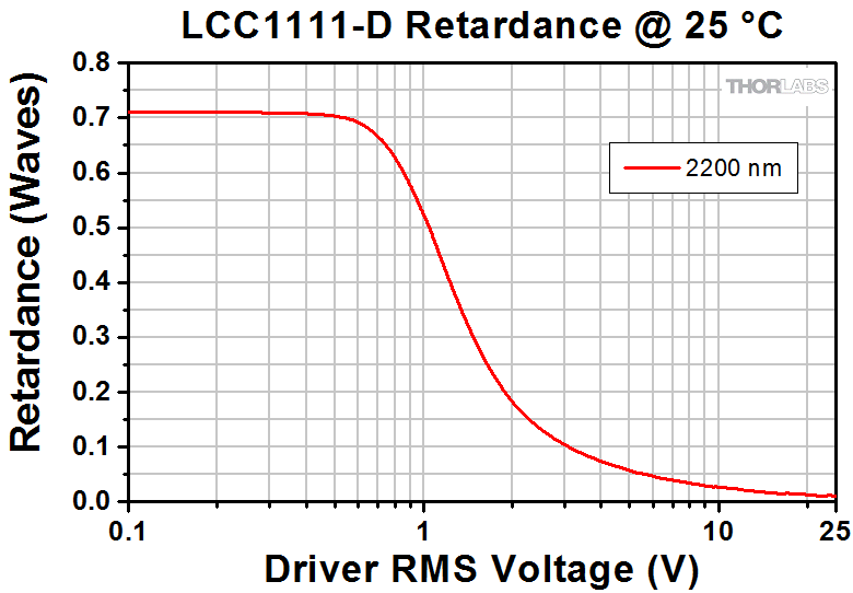 | 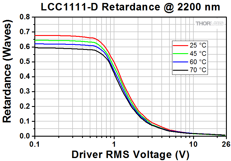 (2200 nm) (2200 nm) | 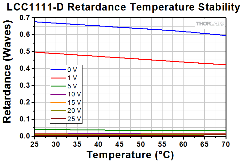 | |
| LCC1111-MIR | 3600 - 5600 nm | 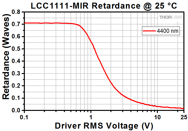 | 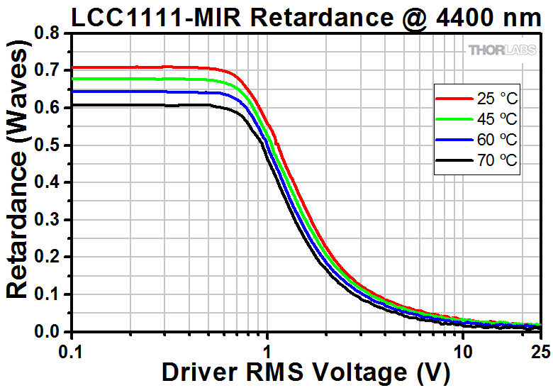 (4400 nm) (4400 nm) | 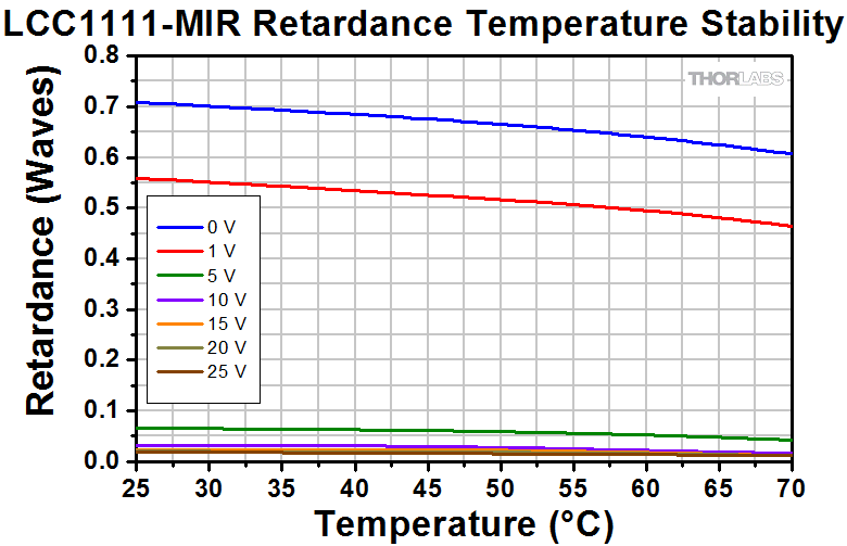 | |
液晶延迟器性能
向列相液晶分子有序排列,分子呈拉伸状,形成光学各向异性。施加电场时,分子沿电场排列,有效延迟量由液晶分子的倾斜控制。为了最大程度地减小材料中离子的影响,液晶设备必须使用交流电驱动。我们的LCC25和KLC101控制器能够最大程度地减少驱动信号中的直流偏压,工作范围从0 V到25 V。
由于分子偏振态的变化,液晶材料会在短波长处表现出较大的色散,在长波长处表现出较小的色散。考虑到这一点,我们在右表中给出每个产品波长范围内一两个波长的延迟量数据。
除此之外,液晶延迟量与仪器的温度相关。随着温度升高,延迟量减小。但从响应时间标签中可以看出,液晶的响应速度在温度较高时有所提高。通常状况下,液晶的折射率(o光和e光)在液晶清亮点温度附近会产生剧烈变化。因此,我们采用高清亮点的材料,以在室温下使用时可将温度依赖性降到最低。
LCC1611 and LCC1511 Fast Switching Ø10 mm LCVR Data
Click Here to Download Retardance Data
Click Here to Download Transmission Data
LCC1111-D and LCC1111-MIR Ø10 mm LCVR Data
Click Here to Download Retardance Data
Click Here to Download Transmission Data
LCC1421 and LCC1221 and LCC1111U Ø10 mm LCVR Data
Click Here to Download Retardance Data
Click Here to Download Transmission Data
*如需规格与LCC1221和LCC1421相同的Ø10 mm LCVR,请联系技术支持techsupport-cn@thorlabs.com。
温度稳定性
液晶延迟器的延迟量会随着温度的升高而略微减少。上表中的曲线图比较了设定驱动电压与温度下的延迟量。对于温度不受控制的环境,推荐使用Thorlabs的温控半波LCR。
LCC1611 and LCC1511 Fast Switching Ø10 mm LCVR Data
Click Here to Download Temperature Stability Data
LCC1111-D and LCC1111-MIR Ø10 mm LCVR Data
Click Here to Download Temperature Stability Data
LCC1421 and LCC1221 and LCC1111U Ø10 mm LCVR Data
Click Here to Download Temperature Stability Data
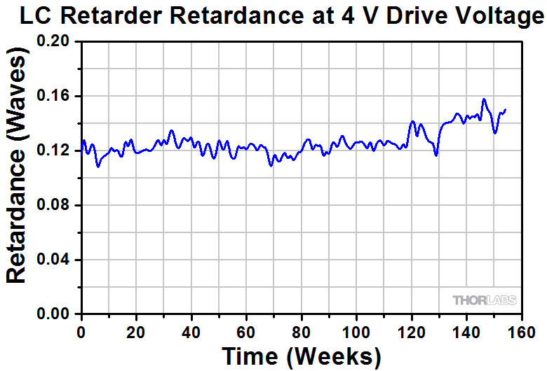
Click to Enlarge
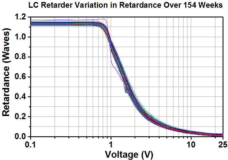
此曲线图显示了154周内延迟量的变化
长期稳定性
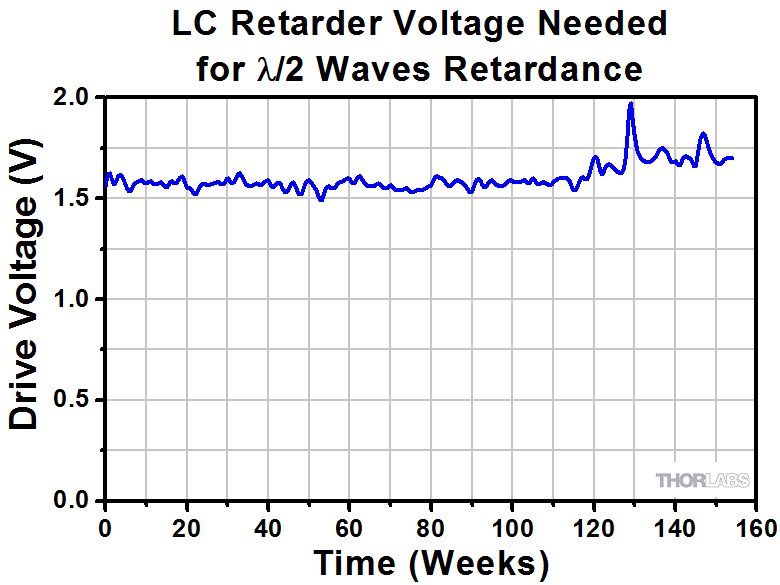
我们的液晶延迟器表现出长期的稳定性能。右图为LCC25液晶控制器驱动上一代LCC1112-A四分之三波液晶延迟器,在154周内延迟量和电压的关系。通过每周的延迟量测试可以看到,延迟量在测试时间内变化非常小。如要获取每周测试的数据,请点击下方下载完整的数据文件。
左下图显示了在同一电压下,延迟量变化微小,而右下图显示在同一延迟量下电压的变化也变化很小。其他型号的延迟器可以得到类似的数据。为了尽量维持延迟器的稳定性能,我们建议一直使用LCC25和KLC101控制器。控制器专为减小直流电压偏移而设计,因此可以最大程度地减少电流累积,实现最大稳定性。

液晶延迟器响应时间
与机械可变波片相比,液晶延迟器没有运动的部件,因此响应时间更短。液晶延迟器的响应时间与很多因素相关,一些是由生产过程决定的,另一些则是由用户决定的。
通常状况下,液晶延迟器在高驱动电压下比在低驱动电压下的响应更快。而且,当LC延迟器在两种电压之间切换时,下降时间(从低电压到高电压)比上升时间(从高电压到低电压)更快。右图为在1.26 V和10 V之间切换电压的示例。如果需要更快的响应速度,我们建议将延迟器与固定波片结合使用,这样就可以在高电压下使用延迟器。请不要超过规格标签中给出的最高电压。
此外,材料粘度和受粘度影响的响应速度同样取决于液晶材料的温度。如下所示,加热液晶延迟器可使响应速度上升两倍之快。我们标准版液晶延迟器的工作温度最高50 °C,依然可以保持指定的延迟量。如果需要更快的速度,延迟器可在最高70 °C下工作,但最大延迟量要减少。
响应速度也与液晶延迟器的厚度、液晶材料的旋转粘度和介电各向异性相关。但是,由于每个变量都会影响其他工作参数,因此,我们的液晶延迟器是优化整体性能的设计,且更强调响应时间。我们同样提供优化其他参数的定制和OEM液晶延迟器,以及更快的液晶延迟器。详情请看上面的定制能力标签,或联系技术支持techsupport-cn@thorlabs.com。
不同温度下样品的响应时间
响应时间的测试是通过将液晶延迟器保持在特定温度,测量从V1至V2的上升时间和从V2至V1的下降时间。V1在所有测试过程中均设为10 V,而V2是指延迟器在最大延迟量(1/2 λ)时的电压。请注意,电压较低时(例如V1 = 5 V)的响应时间比下面指定的响应时间要长。
有补偿的延迟器
| LCC1611-A (AR Coating: 350 - 700 nm) | ||||
|---|---|---|---|---|
| Temperature | V1 | V2 | Rise Time | Fall Time |
| 25 °C | 10 | 2.00 | 3.34 ms | 0.14 ms |
| 45 °C | 10 | 1.80 | 2.44 ms | 0.10 ms |
| 60 °C | 10 | 1.70 | 1.82 ms | 0.09 ms |
| 70 °C | 10 | 1.50 | 1.33 ms | 0.07 ms |
| LCC1611-B (AR Coating: 650 - 1050 nm) | ||||
|---|---|---|---|---|
| Temperature | V1 | V2 | Rise Time | Fall Time |
| 25 °C | 10 | 1.75 | 4.01 ms | 0.27 ms |
| 45 °C | 10 | 1.60 | 3.14 ms | 0.21 ms |
| 60 °C | 10 | 1.45 | 2.55 ms | 0.16 ms |
| 70 °C | 10 | 1.30 | 2.31 ms | 0.15 ms |
| LCC1611-C (AR Coating: 1050 - 1700 nm) | ||||
|---|---|---|---|---|
| Temperature | V1 | V2 | Rise Time | Fall Time |
| 25 °C | 10 | 1.55 | 22.34 ms | 0.55 ms |
| 45 °C | 10 | 1.40 | 16.32 ms | 0.41 ms |
| 60 °C | 10 | 1.25 | 14.08 ms | 0.35 ms |
| 70 °C | 10 | 1.15 | 13.77 ms | 0.31 ms |
| LCC1421-Aa (AR Coating: 350 - 700 nm) | ||||
|---|---|---|---|---|
| Temperature | V1 | V2 | Rise Time | Fall Time |
| 22 °C | 10 | 1.18 | 15.8 ms | 260 µs |
| 45 °C | 10 | 1.02 | 8.56 ms | 176 µs |
| 60 °C | 10 | 0.9 | 7.39 ms | 122 µs |
| 70 °C | 10 | 0.8 | 6.42 ms | 106 µs |
| LCC1421-Ba (AR Coating: 650 - 1050 nm) | ||||
|---|---|---|---|---|
| Temperature | V1 | V2 | Rise Time | Fall Time |
| 22 °C | 10 | 1.26 | 34 ms | 360 µs |
| 45 °C | 10 | 1.16 | 19.6 ms | 243 µs |
| 60 °C | 10 | 1.10 | 15.1 ms | 123 µs |
| 70 °C | 10 | 1.02 | 12.6 ms | 101 µs |
| LCC1421-Ca (AR Coating: 1050 - 1700 nm) | ||||
|---|---|---|---|---|
| Temperature | V1 | V2 | Rise Time | Fall Time |
| 25.6 °C | 10 | 1.00 | 152 ms | 510 µs |
| 45 °C | 10 | 0.80 | 79.1 ms | 326 µs |
| 60 °C | 10 | 0.70 | 59.1 ms | 195 µs |
| 70 °C | 10 | 0.50b | 56.1 ms | 189 µs |
- Ø10 mm通光孔径的有补偿液晶延迟器及响应时间可联系技术支持techsupport-cn@thorlabs.com提供。
- 温度超过70 °C可能无法实现指定的λ/2半波延迟量,这里的V2值对应测量的最大延迟量。
无补偿的延迟器
| LCC1511-A (AR Coating: 350 - 700 nm) | ||||
|---|---|---|---|---|
| Temperature | V1 | V2 | Rise Time | Fall Time |
| 25 °C | 10 | 1.90 | 2.72 ms | 0.16 ms |
| 45 °C | 10 | 1.85 | 2.01 ms | 0.11 ms |
| 60 °C | 10 | 1.70 | 1.53 ms | 0.09 ms |
| 70 °C | 10 | 1.60 | 1.25 ms | 0.07 ms |
| LCC1511-B (AR Coating: 650 - 1050 nm) | ||||
|---|---|---|---|---|
| Temperature | V1 | V2 | Rise Time | Fall Time |
| 25 °C | 10 | 2.05 | 3.41 ms | 0.24 ms |
| 45 °C | 10 | 1.90 | 2.64 ms | 0.19 ms |
| 60 °C | 10 | 1.70 | 1.98 ms | 0.15 ms |
| 70 °C | 10 | 1.55 | 1.89 ms | 0.11 ms |
| LCC1511-C (AR Coating: 1050 - 1700 nm) | ||||
|---|---|---|---|---|
| Temperature | V1 | V2 | Rise Time | Fall Time |
| 25 °C | 10 | 1.65 | 21.29 ms | 0.50 ms |
| 45 °C | 10 | 1.55 | 14.8 ms | 0.41 ms |
| 60 °C | 10 | 1.40 | 12.67 ms | 0.30 ms |
| 70 °C | 10 | 1.30 | 10.8 ms | 0.23 ms |
| LCC1111U-A, LCC1221-Aa (AR Coating: 350 - 700 nm) | ||||
|---|---|---|---|---|
| Temperature | V1 | V2 | Rise Time | Fall Time |
| 25 °C | 10 | 1.12 | 9.8 ms | 0.24 ms |
| 45 °C | 10 | 1.09 | 6.89 ms | 0.2 ms |
| 60 °C | 10 | 0.96 | 5.12 ms | 0.18 ms |
| 70 °C | 10 | 0.91b | 4.98 ms | 0.17 ms |
| LCC1111U-B, LCC1221-Ba (AR Coating: 650 - 1050 nm) | ||||
|---|---|---|---|---|
| Temperature | V1 | V2 | Rise Time | Fall Time |
| 25 °C | 10 | 1.38 | 19.52 ms | 0.44 ms |
| 45 °C | 10 | 1.36 | 10.87 ms | 0.20 ms |
| 60 °C | 10 | 1.32 | 8.54 ms | 0.12 ms |
| 70 °C | 10 | 1.24 | 7.78 ms | 0.10 ms |
| LCC1221-Ca (AR Coating: 1050 - 1700 nm) | ||||
|---|---|---|---|---|
| Temperature | V1 | V2 | Rise Time | Fall Time |
| 25.6 °C | 10 | 1.00 | 95.8 ms | 1.18 ms |
| 45 °C | 10 | 0.90 | 66.4 ms | 1.16 ms |
| 60 °C | 10 | 0.90 | 49.7 ms | 692 µs |
| 70 °C | 10 | 0.10b | 47.2 ms | 671 µs |
| LCC1111-D (AR Coating: 1650 - 3000 nm) | ||||
|---|---|---|---|---|
| Temperature | V1 | V2 | Rise Time | Fall Time |
| 25.6 °C | 10 | 0.99 | 192 ms | 1.0 ms |
| 45 °C | 10 | 0.92 | 80 ms | 0.8 ms |
| 60 °C | 10 | 0.88 | 50 ms | 0.5 ms |
| 70 °C | 10 | 0.86 | 44 ms | 0.2 ms |
| LCC1111-MIR (AR Coating: 3600 - 5600 nm) | ||||
|---|---|---|---|---|
| Temperature | V1 | V2 | Rise Time | Fall Time |
| 25.6 °C | 10 | 1.14 | 372 ms | 14 ms |
| 45 °C | 10 | 1.05 | 204 ms | 6.9 ms |
| 60 °C | 10 | 0.99 | 180 ms | 3.6 ms |
| 70 °C | 10 | 0.94 | 150 ms | 1.6 ms |
上图显示了慢轴和快轴
对准
未施加电压时,液晶延迟器的慢轴对应液晶分子的长轴取向。加上电压后,液晶分子的取向旋转出图示的平面,改变延迟量。Thorlabs的液晶延迟器是向列相液晶装置,必须在交流电下使用,以防离子和自由电荷的累积,从而避免性能下降,仪器烧坏。
为了精确对准液晶盒的轴,先将延迟器安装在合适的旋转安装座上(例如,用于Ø10 mm通光孔径延迟器的RSP1或CRM1P,或用于Ø20 mm通光孔径延迟器的RSP2(/M)或LCRM2A(/M)。然后用探测器或功率计测量光束穿过一对正交线性偏振片后的透过率。接着,将液晶延迟器放在两块正交放置的偏振片之间,慢轴对准第一个偏振片的传输轴。然后缓慢旋转直到透过强度最小。在这种配置中,LC延迟器用于相位调制应用。
如要用作光强调制器或快门,先找到上面所述的最小透射强度。然后将延迟器旋转±45°。对于大多数LC延迟器而言,这个操作会使通过正交偏振片(例如,零级四分之一波片或半波片)透射强度达到最大。但是,考虑到延迟量的波长依赖性,这种规律对于使用宽带光源的多波相位延迟器并不太有效。
应用
采用液晶可变延迟器的偏振控制
液晶可变延迟器(LCVR)可以在宽波长范围内用作可变零级波片。LCVR的光轴定义为没有给液晶盒施加电压时液晶分子的主轴方向,此时的液晶分子是根据液晶取向膜对准的。使用LCVR控制光束的偏振时,应将线偏振入射光的偏振轴方向调至与LCVR的光轴夹角为45°,这样可以让光学元件的动态范围最大。下面给出了随着延迟量减小(RMS电压增大),出射光的偏振态变化示意图。

采用液晶可变延迟器作为纯相位延迟器
为了只影响入射光束的相位,必须使得线偏振入射光的偏振轴对准液晶延迟器的光轴。随着Vrms增大,光束的相位偏移减小。纯相位延迟器经常用于干涉仪,以改变干涉仪其中一个干涉臂相对另一个臂的光程长。采用LCVR可以主动进行控制。
| Damage Threshold Specifications | ||
|---|---|---|
| Item # Suffix |
Laser Type | Damage Threshold |
| -A | Pulsed (ns) | 1.0 J/cm2 (532 nm, 10 Hz, 8 ns, Ø200 µm) |
| Pulsed (fs) | 0.01 J/cm2 (532 nm, 100 Hz, 76 fs, Ø162 µm) | |
| -B | Pulsed (ns) | 1.7 J/cm2 (810 nm, 10 Hz, 7.6 ns, Ø234 µm) |
| Pulsed (fs) | 0.01 J/cm2 (800 nm, 100 Hz, 36.4 fs, Ø189 µm) | |
| -C | Pulsed (ns) | 1.2 J/cm2 (1542 nm, 10 Hz, 10 ns, Ø458 µm) |
| Pulsed (fs) | 0.08 J/cm2 (1550 nm, 100 Hz, 70 fs, Ø145 µm) | |
| -D | Pulsed (ns) | 0.041 J/cm2 (2000 nm, 10 Hz, 6.5 ns, Ø292 µm) |
| Pulsed (fs) | 0.025 J/cm2 (2000 nm, 100 Hz, 100 fs, Ø220 µm) | |
Damage Threshold Data for Thorlabs' Liquid Crystal Variable Retarders
The specifications to the right are measured data for Thorlabs' Liquid Crystal Variable Retarders.
激光诱导损伤阈值教程
以下简要介绍如何测量激光诱导损伤阈值,以及如何根据损伤阈值规格确定光学元件是否适用于特定应用。在选择光学元件时,理解光学元件的激光诱导损伤阈值(LIDT)是很重要的。光学元件的LIDT很大程度上取决于您所使用的激光类型。连续波(CW)激光一般通过热效应(膜层或基底的吸收)引起损伤。脉冲激光通常在引起热损伤之前就会夺去光学元件晶格结构中的电子。请注意,这里提供的指南是以室温工作和全新光学元件为前提(即,符合划痕-麻点规格、表面无污染等)。由于光学元件表面上的灰尘或其它微粒会降低损伤阈值,因此我们建议保持光学元件表面清洁,且没有杂质污染。关于清洁光学元件的更多信息,请查看我们的光学元件清洁教程。
测试方法
Thorlabs根据ISO/DIS 11254和ISO 21254标准测试LIDT。
首先,我们将一束低功率/能量光束入射待测光学元件。光学元件的10个位置在激光光束下曝光一段时间(连续激光)或曝光若干个脉冲(特定的脉冲重频)。曝光后,用显微镜(放大率~100X)检测是否存在可见的损伤。记录损伤位置的个数以及对应的功率/能量。接下来,增大或者降低入射光的功率/能量,在光学元件的10个新位置进行曝光。重复以上过程,直到观察到损伤为止。这样,损伤阈值就是光学元件在没有损伤时能够承受的最高功率/能量。下面的直方图为一个BB1-E02反射镜的测试结果。
上图为带保护层的铝膜反射镜的LIDT测试结果。在此测试中反射镜的损伤阈值为0.43 J/cm2 (1064 nm、脉宽10 ns、10 Hz、Ø1.000 mm)。
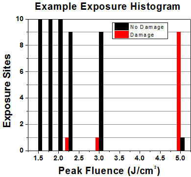
| Example Test Data | |||
|---|---|---|---|
| Fluence | # of Tested Locations | Locations with Damage | Locations Without Damage |
| 1.50 J/cm2 | 10 | 0 | 10 |
| 1.75 J/cm2 | 10 | 0 | 10 |
| 2.00 J/cm2 | 10 | 0 | 10 |
| 2.25 J/cm2 | 10 | 1 | 9 |
| 3.00 J/cm2 | 10 | 1 | 9 |
| 5.00 J/cm2 | 10 | 9 | 1 |
根据测试结果,反射镜的损伤阈值为2.00 J/cm2 (532 nm、脉宽10 ns、10 Hz、Ø0.803 mm)。请注意,这些测试是在干净光学元件上进行的,因为杂质和污染物可能会明显减小元件损伤阈值。本测试结果仅代表某一种膜层,Thorlabs的损伤阈值规格会根据膜层不同而有所变化。
连续波和长脉冲激光
当光学元件被连续波(CW)激光损伤时,通常是由于吸收激光能量造成表面融化或者光学膜层(增透膜)损伤[1]。分析LIDT时,脉宽大于1 µs的脉冲可以看作连续激光。
对于脉宽在1 ns和1 µs之间时,可能由于吸收或介电击穿产生激光诱导损伤,因此用户必须同时分析连续波和脉冲LIDT。吸收可能是由光学元件的固有属性或表面不规则引起的;只有满足或超过制造商提供的表面质量规格的光学元件,LIDT值才有效。尽管很多光学元件能够承受高功率连续波激光,但胶合(如消色差双合透镜)或高吸收(如中性密度滤光片)等光学元件的连续波损伤阈值则较低,这是因为胶合层或金属膜的吸收或散射会降低损伤阈值。
LIDT线性功率密度与脉宽和光斑大小的关系。从长脉冲到连续激光,无论光斑大小,线性功率密度是恒定值。此曲线图由[1]获得。
高脉冲重复频率(PRF)的脉冲激光和连续光束相似。但是,这很大程度上取决于吸收和热扩散等因素,因此没有可靠的方法确定高PRF激光是否会由于热效应损伤光学元件。对于高PRF的光束,其平均功率和峰值功率都必须与同等CW功率比较。此外,对于高度透明的材料,在PRF增加时,LIDT几乎没有或完全没有下降。
为了使用光学元件规定的连续波损伤阈值,有必要了解以下信息:
- 您的激光波长
- 光束直径(1/e2)
- 光束的近似强度轮廓(比如高斯分布)
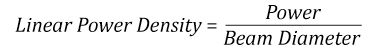
- 光束的线性功率密度(总功率除以1/e2光束直径)
Thorlabs使用W/cm表达CW激光的LIDT值。这样,以线性功率密度给出的LIDT可用于任何光束直径;无需因为光斑大小改变而重新计算,如右图所示。使用下面的公式计算平均线性功率密度。
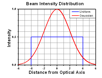
以上计算公式假设是均匀的光束强度轮廓。现在,您必须考虑光束中的热点或其它非均匀强度轮廓,并粗略计算最大的功率密度。例如,高斯光的最大功率密度通常是均匀光束的两倍(如右下图)。
现在,将最大功率密度与光学元件规定的LIDT比较。如果光学元件的测试波长不等于您的工作波长,损伤阈值必须要适当缩放。根据经验,损伤阈值和波长具有线性关系。所以,当波长减小时,损伤阈值也会减小(比如,LIDT在1310 nm时的损伤阈值为10 W/cm,在655 nm时则减小为5 W/cm):
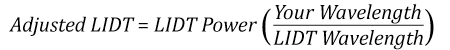
这个经验法则只提供大体的趋势,它不是LIDT和波长的定量分析。比如,对于连续光应用,损伤阈值与膜层和基底的吸收成良好的比例关系,而上述吸收不一定与波长成比例。尽管上述过程对于LIDT计算是较好的经验法则,如果工作波长不同于LIDT波长,请联系技术支持techsupport-cn@thorlabs.com。如果实际功率密度小于调整后的损伤阈值,那么光学元件应该能适用于您的应用。
请注意,我们在网上标定的损伤阈值与我们的测验结果之间存在一定的预留误差,这样就能适应不同批次产品间的差异。如有需要,我们可以提供单独的测试信息和测试证书。我们将使用类似的光学元件进行损伤分析(不会损坏客户的光学元件)。测试可能需要额外费用或交货时间。请联系技术支持techsupport-cn@thorlabs.com获取更多信息。
脉冲激光
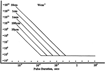
如上所述,脉冲激光一般会对光学元件引入与连续波激光不同类型的损伤。脉冲激光通常不会通过热效应使光学元件产生损伤;而是通过产生能在材料中诱导介电击穿的强电场对其造成损坏。遗憾的是,要将光学元件的LIDT规格与您使用的激光作比较是十分困难的。脉冲激光损坏光学元件有多种机制,并且损坏程度取决于激光脉宽。下表中的高亮部分概括了我们规定的LIDT值对应的脉宽。
小于10-9 s的脉冲与我们规定的LIDT值对比时缺乏可靠性。在这种超短脉冲范围,有各种机制会占主导的损伤机制[2],比如多光子雪崩电离。相反,10-7 s到10-4 s之间的脉冲对光学元件的损伤是由介电击穿或热效应引起的。这意味着连续和脉冲激光的损伤阈值都必须与激光光束进行比较,从而确定光学元件是否适用于您的应用。
| Pulse Duration | t < 10-9 s | 10-9 < t < 10-7 s | 10-7 < t < 10-4 s | t > 10-4 s |
|---|---|---|---|---|
| Damage Mechanism | Avalanche Ionization | Dielectric Breakdown | Dielectric Breakdown or Thermal | Thermal |
| Relevant Damage Specification | N/A | Pulsed | Pulsed and CW | CW |
将特定脉冲激光下给定的LIDT与您使用的激光作对比时,需要了解以下信息:
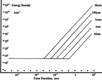
LIDT能量密度与脉冲宽度和光斑大小的关系。对于短脉冲,无论光斑大小,能量密度是恒定值。此曲线图由[1]获得。
- 您的激光波长
- 您的光束能量密度(总能量除以1/e2面积)
- 您的激光脉宽
- 您的激光脉冲重复频率(prf)
- 您的激光的光束直径(1/e2)
- 光束的大致强度分布(如高斯分布)
您的光束能量密度需要以J/cm2计算。右图表明了为何能量密度是短脉冲光源表达LIDT的最佳量度。在这些条件下,以能量密度给出的LIDT与光斑尺寸无关;因此不需要因为光斑大小变化而重新调整LIDT值。计算过程假定光强分布是均匀的。您必须调整能量密度来应对光束中的热点或其他非均匀强度分布,并且粗略计算最大能量密度。例如,高斯光的最大能量密度通常是1/e2光束的两倍。
现在将最大能量密度与光学元件给定的LIDT作比较。如果光学元件测试波长不等于您的工作波长,损伤阈值必须适当缩放[3]。根据经验,损伤阈值和波长比的平方根成比例。所以,当波长减小时,损伤阈值也会减小(比如,在1064 nm时的损伤阈值为1 J/m2,在532 nm时则减小为0.7 J/cm2):
现在您得到了根据波长调整的能量密度,可在接下来的步骤中使用此能量密度。
光束直径在比较损伤阈值时也是很重要的。虽然LIDT在以J/cm²表达时与光斑大小无关;但是大光束可能照射更多的缺陷,这可能会导致更大的激光损伤阈值的变化[4]。对于这里的数据,使用小于1 mm的光束测量LIDT。当光束尺寸大于5 mm时,LIDT(J/cm²)也将和光束直径有关,因为尺寸较大光束容易暴露更多的缺陷。
现在,必须对脉宽进行补偿。脉宽越长,光学元件能承受越多的能量。对于1 ns至100 ns的脉宽,其关系可以近似为:
使用此公式可以根据您的脉宽计算调整LIDT。如果所使用激光的最大能量密度小于调整后的LIDT最大能量密度,光学元件就适用于您的应用。请注意,此计算仅适用于10-9 s和10-7 s之间的脉冲激光。对于10-7 s和10-4 s之间的脉冲激光,您同时还需要考察是否满足连续波LIDT。
请注意,我们在网上标定的损伤阈值与我们的测验结果之间存在一定的预留误差,这样就能适应不同批次产品间的差异。如有需要,我们可以提供单独的测试信息和测试证书。请联系技术支持techsupport-cn@thorlabs.com获取更多信息。
[1] R. M. Wood, Optics and Laser Tech. 29, 517 (1997).
[2] Roger M. Wood, Laser-Induced Damage of Optical Materials (Institute of Physics Publishing, Philadelphia, PA, 2003).
[3] C. W. Carr et al., Phys. Rev. Lett. 91, 127402 (2003).
[4] N. Bloembergen, Appl. Opt. 12, 661 (1973).

为了介绍如何确定某一给定激光系统是否损伤光学元件,下面给出了激光诱导损伤阈值(LIDT)的许多计算实例。为了方便类似的计算,我们提供一个电子表格计算器,可点击右边的按钮下载。使用计算器时,首先在绿色框中输入光学元件指定的LIDT值以及您激光系统的相关参数。电子表格将计算CW和脉冲系统的线性功率密度以及脉冲系统的能量密度值。使用这些数值根据公认的缩放方法为光学元件计算已经调整、按比例缩放的LIDT值。计算器假定高斯光束轮廓,因此必须对其它光束形状引入校正系数(均匀度等等)。LIDT缩放根据经验确定;精度无法保证。注意,在某些光谱区域,光学元件或膜层对激光的吸收能力可能大大降低LIDT。这些LIDT值对于脉宽小于1 ns的超短脉冲无效。

图71A:高斯光束分布的最大光强大约是均匀光束分布的两倍。
CW激光实例
假设一个CW激光系统在1319 nm时输出1/e2直径为10 mm的0.5 W高斯光束。直接用总功率除以光束直径得到光束的平均线性功率密度为0.5 W/cm:
然而,高斯光束的最大功率密度约为均匀光束的最大功率密度的两倍,如图71A所示。因此,系统更准确的最大线性功率密度是1 W/cm。
AC127-030-C消色差双合透镜规定的CW LIDT为350 W/cm,在1550 nm测得。CW损伤阈值通常与激光源的波长直接成比例,因此得出调整的LIDT值:
调整的350 W/cm x (1319 nm / 1550 nm) = 298 W/cm的LIDT值显著高于激光系统的最大线性功率密度,因此系统使用这个双合透镜是安全的。
脉冲纳秒激光实例:不同脉宽的缩放
假设某脉冲Nd:YAG激光系统的三倍频输出355 nm、10 Hz、脉宽为2 ns,单脉冲能量为1 J,并且光束直径为1.9 cm(1/e2)的高斯光束。脉冲能量除以光束面积得到每个脉冲的平均能量密度:
如上所述,高斯光束的最大能量密度约为平均能量密度的两倍。因此,光束的最大能量密度为~0.7 J/cm2。
将这个光束能量密度分别对比BB1-E01宽带介质膜反射镜规定的LIDT值1 J/cm2和NB1-K08 Nd:YAG激光线反射镜的LIDT值3.5 J/cm2。这两个LIDT值都在355 nm下测量,使用脉宽10 ns、重频10 Hz的脉冲激光确定。因此,需要对系统的更短脉宽进行调整。如上一个标签中的描述,纳秒脉冲的LIDT值与激光脉宽的平方根成比例:
使用这个调节因子,BB1-E01宽带反射镜的LIDT值变为0.45 J/cm2,Nd:YAG激光线反射镜的LIDT值变为1.6 J/cm2,将它们直接和光束的0.7 J/cm2最大能量密度比较 。宽带反射镜很可能受到激光损伤,但是特殊的激光线反射镜能够用于激光系统。
脉冲纳秒激光实例:不同波长的缩放
假设某脉冲激光系统以2.5 Hz发射10 ns脉冲,每个脉冲在1064 nm的能量为100 mJ,1/e2光束直径为16 mm,我们现在需要用中性密度滤光片进行衰减。对于高斯输出,使用这些规格计算最大能量密度为0.1 J/cm2。
对于355 nm的10 ns脉冲,NDUV10A Ø25 mm、OD 1.0的反射型中性密度滤光片的损伤阈值是0.05 J/cm2,而对于532 nm的10 ns脉冲,类似的NE10A吸收型滤光片的损伤阈值是10 J/cm2。根据上一个标签中的描述,对于纳秒脉冲,光学元件的LIDT值与波长的平方根成比例:
根据这个比例,反射型滤光片调整后的LIDT值为0.08 J/cm2,吸收型滤光片为14 J/cm2。在这种情况下,为了防止光学损伤,吸收型滤光片是最佳选择。
脉冲微秒激光实例
考虑产生1 µs脉冲的激光系统,单脉冲能量为150 µJ,重频为50 kHz,这将导致5%相对高的占空比。系统处于CW与脉冲激光诱导损伤之间,可能通过任何一种机制引起光学元件损伤。因此,CW和脉冲LIDT值必须同时和激光系统的性质进行对比,以确保安全工作。
如果这个较长脉冲激光器发射980 nm、1/e2直径为12.7 mm的的高斯光束,那么激光输出的线性功率密度为5.9 W/cm,单脉冲能量密度为1.2 x 10-4 J/cm2。将这个值与WPQ10E-980聚合物零级四分之一波片的LIDT值对比,对于810 nm连续波为5 W/cm,对于810 nm的10 ns脉冲为5 J/cm2。与前面一样,光学元件的CW LIDT与激光波长呈线性比例,所以在980 nm时经过调整的CW值为6 W/cm。另一方面,脉冲LIDT与激光波长平方根和脉宽平方根成比例,所以对于1 µs脉冲在980 nm下经过调整的值为55 J/cm2 。光学元件的脉冲LIDT显著大于激光脉冲的能量密度,因此单脉冲不会损伤波片。然而,激光系统的平均线性功率密度较高,和高功率CW光束相似,可能会对光学元件造成热损伤。
上一代Ø10 mm半波液晶延迟器作为特制品提供
下表列出了现版和旧版Ø10 mm半波液晶延迟器。下表中列出的旧版Ø10 mm延迟器可联系技术支持techsupport-cn@thorlabs.com获取。
| Half-Wave Ø10 mm Compensated LC Retarders | ||||
|---|---|---|---|---|
| Wavelength Range | Current Generation | Previous Generation | ||
| Item # | Switching Time (Rise/Fall) | Item # | Switching Time (Rise/Fall) | |
| 350 - 700 nm | LCC1611-A | 3.34 ms / 0.14 ms @ 25 °C, 635 nm | LCC1411-A | 15.8 ms / 260 µs @ 22 °C, 635 nm |
| 650 - 1050 nm | LCC1611-B | 4.01 ms / 0.27 ms @ 25 °C, 780 nm | LCC1411-B | 34.0 ms / 360 µs @ 22 °C, 780 nm |
| 1050 - 1700 nm | LCC1611-C | 22.34 ms / 0.55 ms @ 25 °C, 1550 nm | LCC1411-C | 152 ms / 510 µs @ 25.6 °C, 1550 nm |
| Half-Wave Ø10 mm Uncompensated LC Retarders | ||||
|---|---|---|---|---|
| Wavelength Range | Current Generation | Previous Generation | ||
| Item # | Switching Time (Rise/Fall) | Item # | Switching Time (Rise/Fall) | |
| 350 - 700 nm | LCC1511-A | 2.72 ms / 0.16 ms @ 25 °C, 635 nm | LCC1111-A | 10.2 ms / 310 µs @ 22 °C, 635 nm |
| 650 - 1050 nm | LCC1511-B | 3.41 ms / 0.24 ms @ 25 °C, 780 nm | LCC1111-B | 31.3 ms / 704 µs @ 25.6 °C, 780 nm |
| 1050 - 1700 nm | LCC1511-C | 21.29 ms / 0.50 ms @ 25 °C, 1550 nm | LCC1111-C | 95.8 ms / 1.81 ms @ 25.6 °C, 1550 nm |
 Click to Enlarge
液晶晶盒封装应用
Thorlabs定制液晶器件的能力
Thorlabs提供各种各样的液晶延迟器,包括通光孔径为Ø10 mm或Ø20 mm的1/2、3/4和全波型延迟器,以及1/2波温度控制延迟器。同时,我们也提供OEM和定制延迟器。延迟量范围、镀膜、摩擦角、温度稳定性和尺寸都可以定制,以满足各种特殊光学设计的要求。我们还提供其它定制液晶器件,比如,空的液晶盒、偏振旋转器和噪声衰减器。如需了解更多关于定制液晶器件的信息,请联系Thorlabs技术支持techsupport-cn@thorlabs.com。
我们的工程师会直接与用户讨论定制液晶延迟器所需的规格和其它设计细节。他们将会同时对设计和可行性进行分析,确保能够及时生产出高质量标准的定制产品。
聚酰亚胺(PI)膜和摩擦 - 定制对准角度
向列相液晶分子会自然对准到一个平均方向,结合液晶分子的拉伸状态,可以产生光学各向异性,或方向相关的光学效应。在不施加电压的情况下,液晶盒中的液晶分子方向取决于取向膜,这是一层聚酰亚胺(PI)膜,通过摩擦在膜上产生摩擦角。摩擦产生凹槽,液晶分子就是通过这些凹槽对准的。用户可以通过设定摩擦角选择液晶分子的初始取向。
 Click to Enlarge
定制的无外壳液晶盒
 Click to Enlarge
在真空气室中填充液晶盒
定制液晶盒间隔
液晶盒中的盒体间隔确定了液晶材料的厚度,可以在制造过程中定制。液晶盒的延迟范围与液晶材料的厚度相关:
![]()
 Click to Enlarge
定制液晶盒的测试设备
 Click to Enlarge
定制液晶盒的测试结果
其中,δ为延迟量,d为液晶材料的厚度,λν为光波长,Δn为所使用液晶材料的双折射值。因此,对于给定的波长,延迟量是由液晶盒中的盒体间隔(即液晶层的厚度)决定的。我们提供λ/2到30 nm、3λ/4到30 nm和λ到30 nm的标准延迟范围,但更高的延迟范围也可以定制。
定制液晶材料
用户还可以提供自己准备好的液晶材料,Thorlabs将会用它们来填充到液晶盒中。由于不同的液晶材料具有不同的双折射值,因此不同液晶材料会产生不同的延迟范围。
温度控制/响应时间
温度传感器可以集成到液晶可调延迟器中。通过使用温度控制器,延迟器的温度可以主动稳定在±0.1 °C的变化范围内。液晶材料的粘度在高温下会变低,使延迟器在粘度降低的情况下从一个状态转换到另一个状态。主动温控系统可以用于加热延迟器,以便以更快的响应速度工作。
组装/外壳
如有需要,我们可以定制无外壳的液晶延迟器。
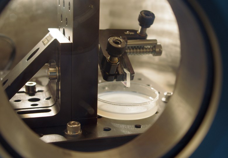
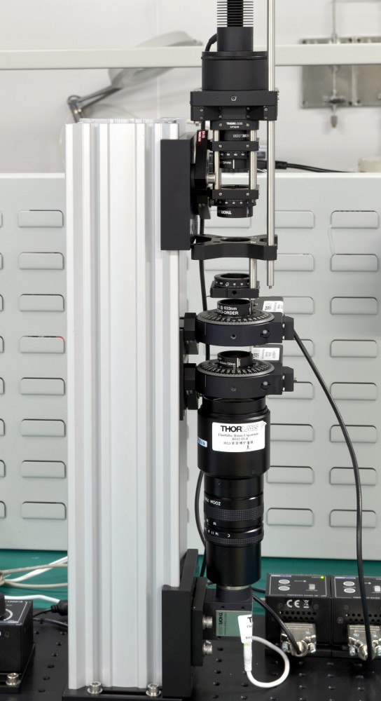
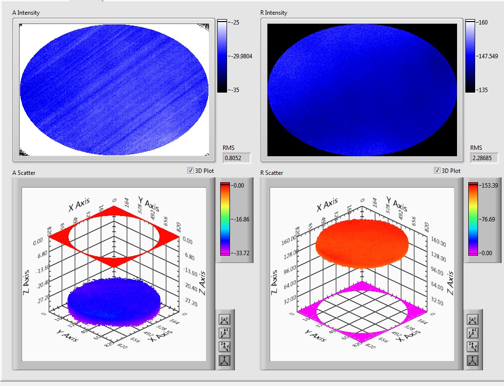
测试
每个液晶延迟器都要测试双折射、均匀度和快轴角度,使用的测量设备如左图所示。设备通过波片和CCD相机测量二维双折射率分布。右图显示了液晶延迟器的样本测试结果,呈现出优异的均匀度。
更多信息
请联系Thorlabs技术支持techsupport-cn@thorlabs.com,了解更多关于我们定制液晶器件或下单的信息。
| Custom Capability | Custom Specification |
|---|---|
| Patterned Retarder Size | Ø100 µm to Ø2" |
| Patterned Retarder Shape | Any |
| Microretarder Size | ≥Ø30 µm |
| Microretarder Shape | Round or Square |
| Retardance Range @ 632.8 nm | 50 to 550 nm |
| Substrate | N-BK7, UV Fused Silica, or Other Glass |
| Substrate Size | Ø5 mm to Ø2" |
| AR Coating | -A: 350 - 700 nm -B: 650 - 1050 nm -C: 1050 - 1700 nm |
点击放大
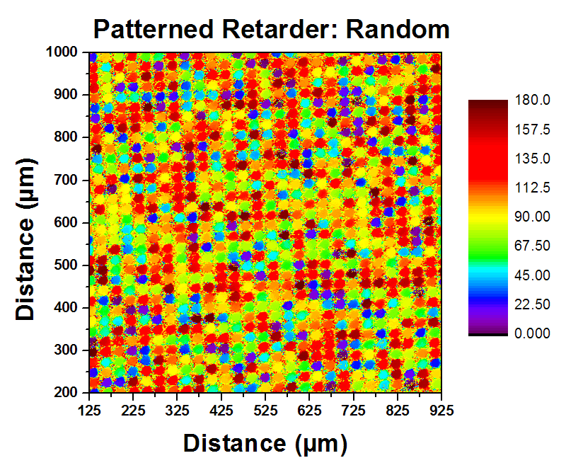
图97A:随机分布的图案化延迟器
特性
- 构建定制微阵列延迟器
- 可以定制尺寸、形状和基底材料
- 延迟范围:50 – 550 nm
- 快轴分辨率:< 1°
- 低于30 nm时延迟有波动
应用
- 3D显示
- 偏振成像
- 衍射光学应用:偏振光栅、偏振测定和光束转向控制
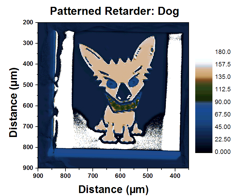
Thorlabs可以定制图案化延迟器,图案尺寸范围从Ø100 µm至Ø2英寸,基底尺寸从Ø5 mm到Ø2英寸。定制的延迟器由微延迟器阵列组成,每个微延迟器的快轴与相邻微延迟器的对准角度不同。微延迟器的尺寸和形状也可以定制。尺寸可以小至30 µm,形状包括圆形和方形。通过控制各个微延迟器的尺寸和形状,以构建具有各种图案化延迟器的大阵列,从而满足几乎所有实验或设备的需求。
这些图案化延迟器由液晶和液晶聚合物构成。我们利用光取向技术,将每个微延迟器的快轴以1°之内的分辨率固定到任何角度。图97A、97B和97C为我们图案化延迟器的实例。这些图呈现了成像偏振仪拍摄的图案化延迟器的测量结果,并表明我们可以明确且单独控制单个微延迟器的快轴取向。
图案化延迟器的制程完全由内部控制。首先制备基底,基底通常是N-BK7或UV熔融石英(虽然也兼容其它玻璃基底)。接着,在基底上镀一层光取向材料,并将基底置于图案化延迟器系统中,暴露在线性偏振光下,以设定微延迟器的快轴。暴露部分的区域取决于微延迟器所需的尺寸;快轴可以以小于1°的分辨率设定在0°与180 °之间。设定完成后,镀上液晶聚合物并用UV光固化,以构造液晶盒。
Thorlabs的LCP消偏器是图案化延迟器的一个实例。理论上,一个真正随机的图案就可以用作消偏器,因为它可以在空间上扰乱入射偏振态。但是,这样的图案也会产生大量衍射。对于我们的消偏器,我们设计了一种线性变化的快轴角度和延迟量,可以对宽带光束和直径小于0.5 mm的单色光束进行消偏,同时不引入额外的衍射。更多详情,请见我们的LCP消偏器页面。
如果向Thorlabs提供所需图案化延迟器的图纸,或者快轴分布的excel文件,我们可以为您构造几乎任何图案化延迟器。欲了解更多关于构建图案化延迟器的信息,请联系技术支持techsupport-cn@thorlabs.com。

点击放大
图97B:螺旋分布的图案化延迟器
点击放大
图97C:图像分布的图案化延迟器
KLC101软件
版本1.0.0
GUI界面用于通过PC控制KLC101液晶控制器。下载请点击下方按钮。
LCC25软件
版本4.0.0
GUI界面用于通过PC控制LCC25液晶控制器。下载请点击下方按钮。
| Posted Comments: | |
Gwan Woo Lee
(posted 2025-04-28 16:53:12.943) Is this product suitable for changing the polarization from 's' to 'p' or vice versa (making it orthogonal)? cdolbashian
(posted 2025-05-01 11:56:11.0) Thank you for contacting Thorlabs! To switch between S and P polarization, a half-wave plate with its optical axis at 45° to the incident polarization axis is required. Our liquid crystal half-wave variable retarders provide >λ/2 retardation, enabling polarization switching when the retardance of the wave plate is set to λ/2 regarding the incident wavelength and the polarization axis of the incident light is oriented at 45° to the optical axis of the retarder. Frank Wu
(posted 2025-04-05 19:01:31.923) Hi,
I couldn't see product information on LCC - MIR series. May I ask if the product is discontinued.
Regards,
Frank Yingliang Liu
(posted 2023-03-15 17:20:02.45) in our setup,we would like to rotate this liquid crystal half wave plate. we have fiound that the pointing direction of the laser has been changed after passing it. Is this normal? or there is a problem with the one we received from you.
By the way, have you considering this effect when you manufacturing this product? is there a way to get rid of the deviation the the beam direction after passing this wave plate when rotating it. For me, It seems that the front surface of this plate is not parallel withthe back surface. cdolbashian
(posted 2023-04-03 02:13:15.0) Thank you for contacting Thorlabs. Our half-wave liquid crystal variable retarders can actively control the phase delay or the polarization state of the light by applying a voltage to the liquid crystal cell. We don't need to rotate the retarder when using it, and the absence of moving parts provides quick switching times on the order of milliseconds. As for the beam deviation, we state it is less than 5 arcmin in the spec. We'll reach out to you via email to discuss your application. Jong-Min Yoon
(posted 2021-04-21 21:34:13.73) Hello
I'm Jong-Min Yoon from Samsung Electronics
I want ask some questions about LCC1411-C
We want to change polarization of our fs-laser source, whose specifications are in below
- Center Wavelength :1560 nm
- Avg. Power : 20 mW
- pulse width : ~100 fs
We will consider that the input power densitiy is not exceed the product's demage threshold spec.
But there seems no dispersion characteristic, so we cannot expect that how much of our laser pulse width(~100fs) will be broaden after LCC1411-C
Could you share us information about dispersion characteristics for LCC1411-C?
Really appreciate for your help to us
Best Regards
Jong-Min YLohia
(posted 2021-04-26 02:19:17.0) Hello Jong-Min, thank you for contacting Thorlabs. Unfortunately, we do not have good characterization data on the dispersion of LC layer but, in theory, it is expected to be quite flat around IR region. The glass substrate is significantly thicker than the LC layer (7 mm of fused silica). Please see this page for the Sellmeier Equation for UVFS: https://www.thorlabs.com/newgrouppage9.cfm?objectgroup_id=6973 Tom Sosnowski
(posted 2019-10-25 18:47:59.353) I'd like to know the average power handling capability of these LC waveplates. How many W/cm^2? YLohia
(posted 2019-10-31 02:47:33.0) Thank you for contacting Thorlabs. We currently provide nanosecond laser damage threshold on this page. Unfortunately, we have not yet performed extensive damage threshold characterization for CW lasers yet. We have reached out to you directly to gather more information about your specific laser and the feasibility of using it with the LCC1221-B. Martin Kozák
(posted 2019-07-08 04:17:54.907) Dear Madam/Sir,
I am searching for a device allowing phase modulation between 0 and PI of a laser beam at 1030 nm at a frequency DC-100 Hz. Do I understand it correctly that the liquid crystal controller LCC25 can drive the modulation at the frequency supplied by an external source? What is the highest modulation frequency, which can be reached for LCC1111-B? I guess that it is limited by the switching time, but this changes quite drastically with temperature and with voltage V1.
Thank you for your reply,
Martin Kozak nbayconich
(posted 2019-07-19 05:21:16.0) Thank you for contacting Thorlabs. That is correct, the LCC25 can be modulated by an external device or the LCC25 can be internally modulated. The rate at which the LC device is modulated will depend on the desired retardance range and applied voltage which determines the switching time of the device. As of now we've measured the rise time to be 14.4ms and the fall time to be 198µs at 70 degrees celsius for the LCC1111-B.
At higher driving voltages you can achieve a shorter switching time however in this case the LCC25 is limited to 25 volts max. The current measured swithcing time at 70 degrees celsius indicates this device may not be suitable for 100hz, if faster switching speeds are desired then you could use the LC retarder in combination with a fixed waveplate and set your V1 voltage at a higher value to reduce the switching time. I will reach out to you directly to discuss your application. user
(posted 2019-05-22 12:36:42.223) Hi,
We would be interested to know the retardance plots of the LCC1221-C for 1064 nm if possible. We would also be interested in the damage thresholds for kHz-1MHz ns, ps and fs pulses if this information is available for the C, B and A products. In addition what would be the custom cost of having the unmounted lambda/2 10 mm retarder coated for C? AManickavasagam
(posted 2019-05-23 07:18:52.0) Response from Arunthathi at Thorlabs: Thanks for your query. I will contact you directly with the requested information. lee.kyeo
(posted 2017-07-15 21:17:46.56) Hi, I found the provided Labview API crashes in Window 10, while calling the "uart_library_win32 (or win64).dll" file.
I tried in both 32- and 64-bit version of Labview 2014 and 2015, and it crashes for all cases.
Since I used the API in Win7 environment for Labview 2014 64-bit, I think the compatibility in Win10 may be an issue. Would you check this problem please? tfrisch
(posted 2017-09-05 03:48:28.0) Hello, thank you for contacting Thorlabs. I will reach out to you directly to troubleshoot this problem you have integrating the controller into LabVIEW. sivathan
(posted 2017-05-22 11:37:52.81) Do you have transmission curves on theses tcampbell
(posted 2017-05-22 02:21:07.0) Response from Tim at Thorlabs: thank you for your feedback. Yes, please see the Performance tab for transmission curves and other performance graphs. parksj003
(posted 2017-03-13 19:31:23.203) Hello,
We are interested in developing polarization-sensitive confocal microscope and trying to install the LCC1111-B in the excitation beam path. I have a question.
The controller (LCC25) seems to produce square wave output with fixed frequency of 2000 Hz. This is may be necessary to minimize effects due to ions in the material. If so, the toggle (flipping) time between positive an native voltages will be also few tens of msec? That means that any measurement between this toggle time gives hugh error?
Best,
Seongjun tfrisch
(posted 2017-03-15 09:10:18.0) Hello, thank you for contacting Thorlabs. The 2000Hz oscillation is to reduce charge buildup. That will be faster than the response of the material, so you would still be limited by the material response time. I will reach out to you directly to discuss this further. parksj003
(posted 2016-12-02 07:18:02.17) Hello,
I would like to use the Half-Wave Liquid Crystal Variable Retarders for our research, but I am wondering that it can be fine if femto-second laser (wavelgnth~700-1000 nm , Power~3W) is used.
Best,
Seongjun tfrisch
(posted 2016-12-05 10:32:55.0) Hello, thank you for contacting Thorlabs. I will reach out to you directly about your application. The response of the liquid crystal will be much slower than a typical fs rep rate. Furthermore, I have concerns about potential damage. julian.robertz
(posted 2016-10-20 15:26:57.877) Dear Thorlabs,
Thank you for so much informations to your products. I found some mistakes on the retardance data. In the excel file is written, that the retardance where measured with a wavelength of 1310nm and 1550nm. But this makes no sense for LC's specified for 350nm up to 700nm.
Can you correct that please. Also please check if the data were correct.
Thank you tcampbell
(posted 2016-10-20 11:11:07.0) Response from Tim at Thorlabs: Thank you for your feedback. You are correct, the retardance data was not specified at the proper wavelengths. We have fixed this in the raw data file. The values in each data set were also checked and corrected as necessary. stu-adysuwardi
(posted 2016-09-21 14:25:03.87) Hello there, for LCC1111-A, may I know what is the maximum AC voltage (peak to peak) that it can withstand?
Will appreciate if data about switching time vs applied voltage (up to maximum allowed voltage) is provided. (the one on the website is only up to 20 V).
I would like to know at 1 kHz and certain applied voltage, even if it is not fully switched, what is the degree of switching? (e.g. 0.xx waves).
Thanks very much in advance. jlow
(posted 2016-09-23 03:48:26.0) Response from Jeremy at Thorlabs: The LC retarder can typically withstand at least 40-50V but we wouldn't recommend it as the lifetime of the LC cell can be affected at high voltages. The response time is related to many factors, such as voltages (especially the end voltage), temperature, operational wavelength and so on. Generally speaking, higher voltage and temperature results in faster speed. We will contact you directly to provide more information specific to your application. tfrisch
(posted 2016-08-25 08:37:07.237) Hello Pierre, thank you for contacting Thorlabs. You are correct that the LC material does not respond on the order of kHz. The kHz signal is to prevent charge buildup. I have contacted you directly. -Tyler at Thorlabs USA drobniak
(posted 2016-07-29 16:35:03.747) Hello, I bought a LCC1111-C retarder and I am trying to understand the working principle of the liquid crystal.
Can you please explain me how the molecules of the crystal produce a phase shift between slow- and fast-axis while working with a frequency around 1kHz? As I understood, the frequency of 1kHz is too fast for the molecules to switch, so what is the process inducing this phase shift?
Thank you. Regards, Pierre Drobniak jbarnes
(posted 2016-04-20 13:28:21.62) I have a question regarding your LCC1111-A retarder. It is mentioned that only an AC voltage can be used to drive the retarder and that the LCC25 voltage controller actively reduces any DC applied to the device. Is the source of this DC from the controller itself, or does a DC potential develop in the LC retarder over time which must be compensated for?
Thank you. Regards, Dr. Jack Barnes besembeson
(posted 2016-04-21 04:02:43.0) Response form Bweh at Thorlabs USA: The source of the DC is from the LC retarder. Due to continuous motion of the liquid crystal molecules when being driven, there is charge build up that could separate and create a DC potential. j.aans
(posted 2015-11-30 12:17:31.797) Hello, is there any data on damage thresholds for 1064nm? Can a CW 3W 10mm diameter beam go through the LCC1111-A without damaging it? Thanks, JB Aans besembeson
(posted 2015-12-02 02:45:43.0) Response from Bweh at Thorlabs USA: We don't have tested data for that wavelength but note that LCC1111-A has an anti-reflection coating to increase throughput in the 350-700nm range, not optimal for your 1064nm wavelength. I would recommend the -C model that has the following CW damage threshold guide: 2.5MW/cm^2 (for 1540nm, CW, 0.018mm diameter). jrg
(posted 2015-08-19 15:37:55.323) I recently purchased 1/2 wave LCD retarders for visible and near-IR. When removed from their original shipping boxes the optical surfaces were protected by adhesive yellow tape (perhaps Kapton or polymide tape) covering the mounting assembly.
I'd like to continue to protect these items when they are not in use. Can you tell me what tape you use?
Thanks -
James Graham jlow
(posted 2015-08-25 03:53:19.0) Response from Jeremy at Thorlabs: The tape we use is the Kapton tape. You can find the tape at http://www.thorlabs.com/newgrouppage9.cfm?objectgroup_id=6809. johnnysheng
(posted 2015-01-30 10:50:46.343) Is the PI layer inorganic?
What is the laser damage threshold at, e.g., 450nm? jlow
(posted 2015-01-30 04:39:18.0) Response from Jeremy at Thorlabs: The PI layer is polyimide, which is organic. We do not have a damage threshold specification for this at the moment. I will contact you directly to discuss about this further. nick.robins
(posted 2015-01-26 22:00:14.677) it appears that this product should work well with a standard function generator. however, we have not managed to get it working. we are using an agilent fg with a 2kHz square wave and the specified voltage range, but the retarder appears unresponsive. we checked very carefully that there was no dc offset on the fg. cdaly
(posted 2015-01-28 01:43:24.0) Response from Chris at Thorlabs: The LCC1111-B has a typical rise and fall time of 16.0 ms / 360 µs. 2 kHz is too fast of a signal for the liquid crystal retarder to respond to. Since it cannot switch fast enough, it will appear unresponsive. Alexander.Radnaev
(posted 2013-12-11 20:04:56.887) Hello, what is the maximum allowed light intensity for this product (damage threshold)?
Thanks,
Alex. jlow
(posted 2014-01-08 10:48:54.0) Response from Jeremy at Thorlabs: We do not have the damage threshold data specifically for the -A version (we are going to be testing this in the near future). The estimated damage threshold is around 500W/cm (532nm). If there are dust, oil, or any contamination on the optic, it can be damaged even with low beam power. cdaly
(posted 2013-02-27 16:17:00.0) Response from Chris at Thorlabs: Thank you for using our web feedback feature. The thickness of the crystal itself is only about 3um. The thickness of the entire optic within the housing is ~6mm, as this 3um crystal sits between two 3mm fused silica substrates. sinclair
(posted 2012-11-05 16:21:31.607) What the the damage thresholds for the visible series liquid crystal retarders? CW lasers, 400-650nm.
Also, do you have any retardance data for 488 and 561nm?
Thanks,
Peter jlow
(posted 2012-10-02 10:42:00.0) Response from Jeremy at Thorlabs: You can control the LCC25 using serial command. This is detailed on pages 9 and 10 in the manual for the LCC25 (found at http://www.thorlabs.com/Thorcat/18800/LCC25-Manual.pdf). ashwin3342
(posted 2012-10-02 07:32:43.0) I want to control my LCC 25 via PC. I have installed National Instruments CVI. Please tell me how to write commands. jlow
(posted 2012-09-04 08:37:00.0) Response from Jeremy at Thorlabs: We have measured the laser damage threshold for the LCC1111-C to be 2.50J/cm^2 (1542nm, 10ns, 10Hz, Ø0.458mm). Unfortunately we do not have data at 1064nm. vssrikanth
(posted 2012-08-24 03:31:27.0) Sir/Madam,
1.We are interested in your device. We were looking for an application where the Polarisation of 1064nm/1572nm needs to be changed from 's' to 'p' i.e., to make it orthogonal.
Please let us know the Peak power density that these devices can withstand for 1064nm, pulse width ~15ns, rep rate ~20pps.
Regards,
Srikanth VS
Mgr., D&E tcohen
(posted 2012-07-18 10:16:00.0) Response from Tim at Thorlabs: The new liquid crystal retarders have much higher optical quality. The main difference is that the new 10mm retarders have significantly better uniformity, lower optical losses and a lower wavefront distortion. Additionally, we have also improved the switching time, operating temperature range and wavelength coverage. nizamov.shawkat
(posted 2012-07-17 12:25:42.0) What is the difference between newer LCC1111 and older LCR-1? Both are 10mm clear aperture half-wave LC retarders, controlled by the same LCC25 controller. But the price is very much different. |

 放大
放大| Key Specificationsa | |||
|---|---|---|---|
| Item # | LCC1611-A | LCC1611-B | LCC1611-C |
| Wavelength Range | 350 - 700 nm | 650 - 1050 nm | 1050 - 1700 nm |
| Retardance Rangeb | 0 nm to >λ/2 | ||
| Switching Time (Rise/Fall, Typical) | 3.34 ms / 0.14 ms @ 25 °C, 635 nm | 4.01 ms / 0.27 ms @ 25 °C, 780 nm | 22.34 ms / 0.55 ms @ 25 °C, 1550 nm |
| Retardance Uniformity (RMS)c | < λ/20 @ 400 nm | < λ/20 @ 650 nm | < λ/20 @ 1050 nm |
| Surface Quality | 60-40 Scratch-Dig | ||
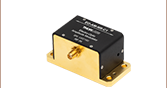
- 通光孔径Ø10 mm
- 延迟量:0 nm到λ/2
- 补偿以实现0 nm的最小延迟量
- 外径1英寸
- 提供3种标准增透膜
Thorlabs有补偿的半波液晶延迟器通光孔径为Ø10 mm,增透膜的适用波长为350 - 700 nm(LCC1611-A)、650 - 1050 nm(LCC1611-B)或1050 - 1700 nm(LCC1611-C)。延迟器内集成的补偿层可以在5 V到20 V之间的特定驱动电压下,实现最小为0 nm的延迟量(更多信息,请看性能标签)。这些延迟器的外径为1英寸,兼容我们所有用于9 mm厚光学元件的Ø1英寸光学安装座。延迟器前正面的刻线表示慢轴。此外,这些已安装的延迟器带有长约930 mm的BNC电线,以便连接电子元件。延迟器具有1英寸外径,可使用RSP1(/M)可安装接杆的旋转安装座或CRM1PT(/M) 30 mm笼式旋转安装座进行安装。
*如果您的应用不需要LCC1611-x LCVR的快速响应,可以联系技术支持techsupport-cn@thorlabs.com获取上一代Ø10 mm通光孔径的延迟器。详情请看定制能力标签。

 放大
放大| Key Specificationsa | |||
|---|---|---|---|
| Item # | LCC1511-A | LCC1511-B | LCC1511-C |
| Wavelength Range | 350 - 700 nm | 650 - 1050 nm | 1050 - 1700 nm |
| Retardance Rangeb | ~30 nm to >λ/2 | ||
| Switching Time (Rise/Fall, Typical) | 2.72 ms / 0.16 ms @ 25 °C, 635 nm | 3.41 ms / 0.24 ms @ 25 °C, 780 nm | 21.29 ms / 0.50 ms @ 25 °C, 1550 nm |
| Retardance Uniformity (RMS)c | < λ/50 @ 400 nm | < λ/50 @ 650nm | < λ/50 @ 1050 nm |
| Surface Quality | 40-20 Scratch-Dig | ||
- 通光孔径Ø10 mm
- 延迟量:~30 nm到λ/2
- 外径1英寸
- 提供3种标准增透膜
Throlabs无补偿的半波液晶延迟器通光孔径Ø10 mm,增透膜的适用波长为350 - 700 nm(LCC1511-A)、650 - 1050 nm(LCC1511-B)或1050 - 1700 nm(LCC1511-C)。这些延迟器的外径为1英寸,兼容我们用于8 mm厚光学元件的Ø1英寸光学安装座。延迟器正面的刻线表示慢轴。此外,这些已安装延迟器带有长930 mm的BNC电缆,用于接电。延迟器具有1英寸外径,可使用RSP1(/M)可安装接杆的旋转安装座或CRM1PT(/M) 30 mm笼式旋转安装座进行安装。
我们也提供带温控的Ø10 mm半波液晶延迟器,可在温度变化的环境下提供恒定的延迟量。
*如果您的应用不需要LCC1511-x LCVR的快速响应,可以联系技术支持techsupport-cn@thorlabs.com获取上一代Ø10 mm通光孔径的延迟器。详情请看定制能力标签。

 放大
放大| Key Specificationsa | ||
|---|---|---|
| Item # | LCC1111-D | LCC1111-MIR |
| Wavelength Range | 1650 - 3000 nm | 3600 - 5600 nm |
| Retardance Rangeb | ~30 nm to >λ/2 | |
| Switching Time (Rise/Fall, Typical) | 192 ms / 1 ms @ 25.6 °C, 2200 nm | 372 ms / 14 ms @ 25.6 °C, 4400 nm |
| Retardance Uniformity (RMS)c | < λ/30 @ 1650 nm | < λ/10 @ 3600 nm |
| Surface Quality | 60-40 Scratch-Dig | |
- 通光孔径Ø10 mm
- 延迟量:~30 nm到λ/2
- 外径1英寸
- 提供2种标准增透膜
Thorlabs无补偿的半波液晶延迟器通光孔径Ø10 mm,增透膜的适用波长为1650 - 3000 nm(LCC1111-D)或3600 - 5600 nm(LCC1111-MIR)。这些延迟器的外径为1英寸,兼容我们用于8 mm厚光学元件的Ø1英寸光学安装座。延迟器正面的刻线表示慢轴。此外,这些已安装延迟器带有长930 mm的BNC电缆,用于接电。延迟器具有1英寸外径,可使用RSP1(/M)可安装接杆的旋转安装座或CRM1PT(/M) 30 mm笼式旋转安装座进行安装。
我们也提供带温控的Ø10 mm半波液晶延迟器,可在温度变化的环境下提供恒定的延迟量。

 放大
放大| Key Specificationsa | ||
|---|---|---|
| Item # | LCC1111U-A | LCC1111U-B |
| Wavelength Range | 350 - 700 nm | 650 - 1050 nm |
| Retardance Rangeb | ~30 nm to >λ/2 | |
| Switching Time (Rise/Fall, Typical) | 9.8 ms / 0.24 ms @ 25 °C, 635 nm | 19.52 ms / 0.44 ms @ 25 °C, 780 nm |
| Retardance Uniformity (RMS)c | < λ/50 @ 400 nm | < λ/50 @ 650 nm |
| Surface Quality | 40-20 Scratch-Dig | |
| Dimensions (L x W x D) | 17.0 mm x 12.0 mm x 6.0 mm (0.67" x 0.47" x 0.24") | |
- 通光孔径Ø10 mm
- 延迟量:~30 nm到λ/2
- 尺寸公差:±0.4 mm
- 增透膜适用于350 - 700 nm或650 - 1050 nm
Thorlabs无补偿的未封装半波液晶延迟器通光孔径Ø10 mm,非常适合空间受限的应用。LCC1111U-A的增透镀膜适用于350 - 700 nm,而LCC1111U-B的增透镀膜适用于650 - 1050 nm。这些延迟器结构紧凑,能够灵活安装或放置在已有系统中,适合OEM或其他特定的应用。LCC1111U-x未安装延迟器带有连接电压驱动的导线,并兼容下面出售的LCC25和KLC101液晶控制器。
可以定制其他波长、通光孔径为Ø10 mm或Ø20 mm的版本。如需定制未封装的延迟器,请联系技术支持techsupport-cn@thorlabs.com。

 放大
放大| Key Specificationsa | |||
|---|---|---|---|
| Item # | LCC1421-A | LCC1421-B | LCC1421-C |
| Wavelength Range | 350 - 700 nm | 650 - 1050 nm | 1050 - 1700 nm |
| Retardance Rangeb | 0 nm to >λ/2 | ||
| Switching Time (Rise/Fall, Typical) | 15.8 ms / 260 µs @ 22 °C | 34 ms / 360 µs @ 22 °C | 152 ms / 510 µs @ 25.6 °C |
| Retardance Uniformity (RMS)c | < λ/20 @ 400 nm | < λ/20 @ 650 nm | < λ/20 @ 1050 nm |
| Surface Quality | 60-40 Scratch-Dig | ||
- Ø20 mm的大通光孔径
- 延迟量:0 nm到λ/2
- 补偿以实现0 nm的最小延迟量
- SM2外螺纹
- 提供3种标准增透膜
Thorlabs有补偿的半波液晶延迟器通光孔径为Ø20 mm,增透膜适用波长为350 - 700 nm(LCC1421-A)、650 - 1050 nm(LCC1421-B)或1050 - 1700 nm(LCC1421-C)。延迟器内集成的补偿层可在5 V到20 V之间的特定驱动电压下,实现0 nm的最小延迟量(更多信息,请看性能标签)。这些延迟器具有SM2外螺纹,兼容我们的Ø2英寸带螺纹的光学元件安装座,其中包括RSP2(SM2安装座,提供精确的旋转调节,且能安装接杆)或LCRM2A(可以安装60 mm笼式组件)。延迟器前面的刻线表示慢轴。此外,这些已安装的延迟器带有长944 mm的BNC电线,以便连接电子元件。

 放大
放大| Key Specificationsa | |||
|---|---|---|---|
| Item # | LCC1221-A | LCC1221-B | LCC1221-C |
| Wavelength Range | 350 - 700 nm | 650 - 1050 nm | 1050 - 1700 nm |
| Retardance Rangeb | ~30 nm to >λ/2 | ||
| Switching Time (Rise/Fall, Typical) | 9.8 ms / 0.24 ms @ 25 °C | 19.52 ms / 0.44 ms @ 25 °C, 780 nm | 95.8 ms / 1.81 µs @ 25.6 °C |
| Retardance Uniformity (RMS)c | < λ/50 @ 400 nm | < λ/50 @ 650 nm | < λ/50 @ 1050 nm |
| Surface Quality | 40-20 Scratch-Dig | ||
- Ø20 mm的大通光孔径
- 延迟量:~30 nm到λ/2
- 外径2英寸
- 提供3种标准增透膜
Throlabs无补偿的液晶延迟器通光孔径Ø20 mm,增透膜的适用波长为350 - 700 nm(LCC1221-A)、650 - 1050 nm(LCC1221-B)或1050 - 1700 nm(LCC1221-C)。这些延迟器外径为2英寸,兼容我们所有用于13 mm厚光学元件的Ø2英寸光学安装座。延迟器正面的刻线表示慢轴。此外,这些已安装的延迟器带有长约940 mm的BNC电线,以便连接电子元件。延迟器具有2英寸外径,可使用RSP2可安装接杆的旋转安装座或LCRM2A 60 mm笼式旋转安装座进行安装。

 放大
放大- 输出方波电压:0至±25 VAC
- LCC25:2000 ± 5 Hz
- KLC101:可调范围为500 Hz至10 kHz
- 内部和外部选项,用于调制输出方波幅度
- 使用设备面板编辑设置或通过PC的USB输入进行控制
LCC25和KLC101液晶(LC)控制器均可用于操作Thorlabs的液晶盒、旋转器和延迟器(除了带集成控制器的LCC2415-VIS)。每个控制器都提供方波AC电压输出,其幅度可以在0 Vrms至±25 Vrms范围内调节。两种控制器都可实时自动探测任何直流偏移,并将其校正到±10 mV以内,这样有助于延长液晶设备的使用寿命。
LCC25台式控制器
LCC25 LC控制器可产生2000 Hz的方波AC电压输出。用户通过前面板和USB接口选择可两种电压电平,即电压1和电压2。LCC25在恒定电压模式下运行时,控制器的输出幅度等于两个设定电压电平其中一个的幅度。在调制模式下,2,000 Hz方波输出的幅度将在电压1和电压2之间切换,其中频率可通过内部设置(0.5 Hz至150 Hz),或通过0至5 V TTL输入外部触发(0.5 Hz至500 Hz)。LCC25控制器的软件还可通过指定起始电压、终止电压、电压步长和驻留时间来定义电压序列。
更多关于此控制器功能的信息,请访问LCC25控制器页面。
KLC101 K-Cube®控制器
KLC101 K-Cube® LC控制器属于Thorlabs高端紧凑型控制器系列产品之一。这款控制器提供方波AC输出电压,其中用户可设置的频率为500 Hz至10 kHz,并且封装尺寸小,仅为60.0 mm x 60.0 mm。控制器可以存储两种电压和频率组合,PresetV1和PresetV2,可选择其中一个作为输出。此外,控制器顶面板、软件和触发端口都可创建自定义输出电压序列。使用顶部面板控件或软件,可将电压设置为以0.1到150 Hz范围内的速率在PresetV1和PresetV2之间切换。在此模式下,其中一个触发端口将输出5 V逻辑信号,高电平指示输出为PresetV2,低电平指示输出为PresetV1。另外,可以将触发端口用作5 V逻辑信号的输入端口,以在PresetV1和PresetV2之间切换。此软件还支持序列和扫描模式。序列工具可用于设置输出电压幅度、频率和步长持续时间的序列。在扫描模式下,KLC101控制器将以用户指定的步长和步长持续时间在用户设置的起始和终止电压之间进行扫描。
请注意,KLC101控制器不附带电源。对于需要单个K-cube的应用,可以使用TPS002电源(下方有售)。我们还提供可与多个K-cube一起使用的USB控制器集线器。
更多关于此控制器功能及其电源选项的信息,请看完整的KLC101控制器页面。
| Item # | Adjustable Output Voltage | Voltage Resolution | Adjustable Output Frequencya | Internal Modulationa | External Modulation | Slew Rate | DC Offset | Warm Up Time | Output Current (Max) | External Input Voltage (Max) |
|---|---|---|---|---|---|---|---|---|---|---|
| LCC25 | 0 to ±25 V RMS | 1.0 mV | 2,000 ± 5 Hz | 0.5 to 150 Hz | 0.5 to 500 Hz | 10 V/µs | ±10 mV | 30 Minutes | 15 mA | 5 VDC |
| KLC101 | 500 Hz to 10 kHz | 0.1 to 150 Hz | 150 Hz (Max) | 50 mA |