 Products Home
Precision Double Slits
- Slit Width: 40, 50, or 100 µm
- Slit Spacing: 3 or 6 Times Slit Width
- 3 mm Slit Length
- Stainless Steel Foils Blackened on Both Sides for Increased Absorbance
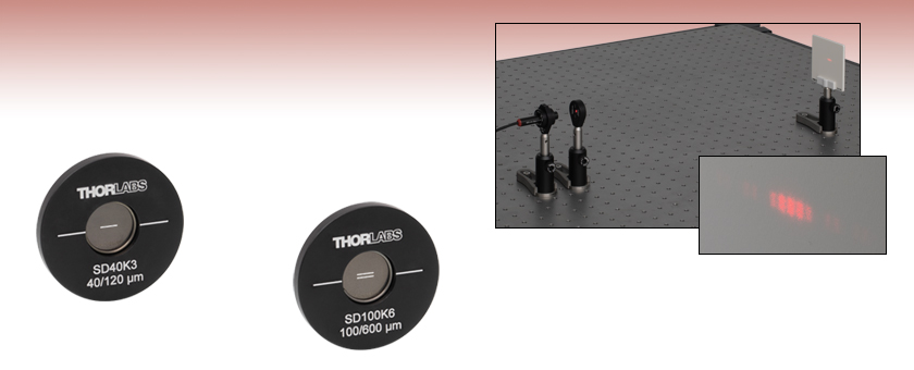
SD40K3
40 µm Slit Width,
120 µm Slit Spacing
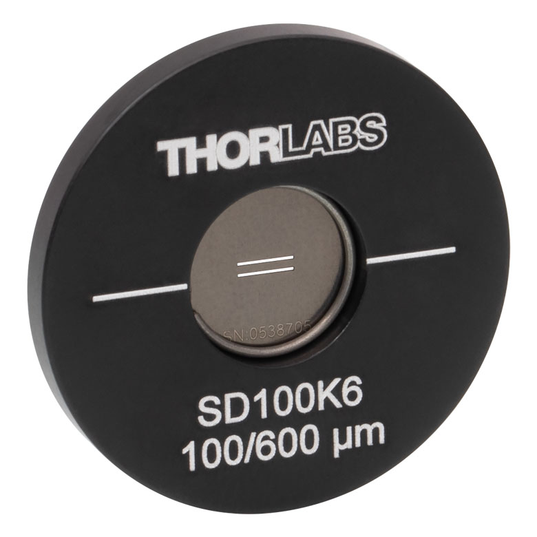
SD100K6
100 µm Slit Width,
600 µm Slit Spacing
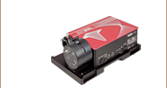
Application Idea
An SD40K3 Double Slit is mounted in the light path of a PL202 Laser. The transmitted interference pattern can be viewed on a screen 50 cm away.
The double slit interference pattern is visible on our EDU-VS2 Viewing Screen.


Please Wait
| Apertures Selection Guide |
|---|
| Single Precision Pinholes |
| Circular in Stainless Steel Foils |
| Circular in Stainless Steel Foils, Vacuum Compatible |
| Circular in Gold-Plated Copper Foils |
| Circular in Tungsten Foils |
| Circular in Molybdenum Foils |
| Square in Stainless Steel Foils |
| Pinhole Kits |
| Pinhole Wheels |
| Manual |
| Motorized |
| Pinhole Spatial Filter |
| Single Slits |
| Double Slits |
| Annular Apertures |
| Alignment Tools |
Click to Enlarge
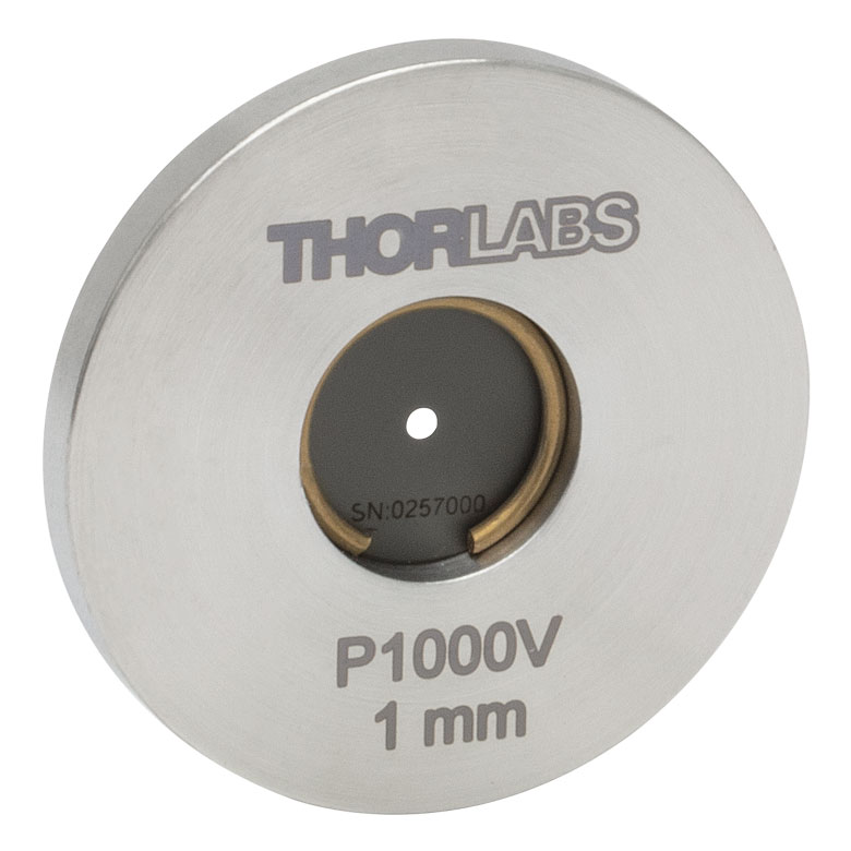
Dimensions for Mounted Stainless Steel Slits in Ø1" Housings
Features
- Precision Double Slits in Stainless Steel Foils Mounted in Ø1" Aluminum Housings
- Black-Anodized Aluminum Housing:
- 1" Outer Diameter, 0.10" Thick
- Includes Engraved Horizontal Lines on the Front Face to Facilitate Slit Alignment
- Slit Widths: 40, 50, or 100 µm
- Slit Spacing: 3X or 6X Slit Width
- Slit Length: 3 mm
- Contact Tech Support to Discuss Custom Options
Thorlabs' Optical Double Slits in blackened stainless steel foils have 3 mm long slits with widths of 40 µm, 50 µm, or 100 µm and are available with a spacing of 3X or 6X the slit width. For example, SD40K3 is a double slit with 40 µm slit width and 120 µm spacing, while SD40K6 is a double slit with 40 µm slit width and 240 µm spacing. To avoid creating interference and diffraction patterns in multiple directions, ensure that the size of the incident beam is smaller than the length (3 mm) of the slit. Foils are mounted in Ø1" aluminum housings.
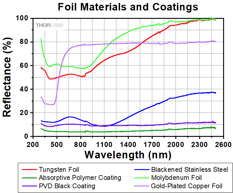
If you do not see what you need in our stocked offerings below, it is possible to special order slits that are fabricated from different substrate materials, have different slit sizes, incorporate multiple slits in one foil, or provide different slit configurations. Low-power applications may benefit more from the absorbance of blackened stainless steel foils. High-power applications may need the high damage threshold and reflectance of gold-plated copper foils, the high melting point and lower reflectance of our tungsten foils, or the high melting point of our molybdenum foils paired with the low reflectance (4% @ 800 nm) of their black-coated front side. Please see the Foil Comparison and Graph tabs for more information. Customized housings are also available. Please contact Tech Support to discuss your specific needs.
| Precision Pinhole and Optical Slit Selection Guide | |||||
|---|---|---|---|---|---|
| Material | Product | ||||
| Blackened Stainless Steel | Circular Precision Pinholes | ||||
| Square Precision Pinholes | |||||
| Optical Slits | |||||
| Stainless Steel with PVD Black Coating |
Circular Precision Pinholes | ||||
| Gold-Plated Copper Foil (Rear) and PVD Black Coating (Front) |
Circular Precision Pinholes | ||||
| Tungsten Foil | Circular Precision Pinholes | ||||
| Molybdenum Foil (Rear) and Absorptive Polymer Coating (Front) |
Circular Precision Pinholes | ||||
Precision Pinholes and Slits
Thorlabs offers precision pinholes with blackened stainless steel, gold-plated copper, tungsten, or molybdenum foils. Our pinholes with stainless steel foils are blackened on both sides for increased absorbance and are available from stock in circles from Ø1 µm to Ø9 mm and squares from 100 µm x 100 µm to 1 mm x 1 mm. Our stainless steel pinholes with a black PVD coating are vacuum compatible and available in 5 μm to 2 mm diameters. Our pinholes with gold-plated copper foils, plated with gold on one side and black PVD coated on the reverse, are available with pinhole diameters from 5 µm to 2 mm. Our pinholes with tungsten foils are uncoated and available with pinhole diameters from 5 µm to 2 mm. Lastly, our pinholes with molybdenum foils have an absorptive polymer coating on the front sides and are available with pinhole diameters from 5 µm to 2 mm. We also offer slits in blackened stainless steel foils from stock with slit widths from 5 to 200 µm.
If you do not see what you need among our stock pinhole and slit offerings, it is also possible to special order pinholes and slits that are made with different foil materials, have different hole sizes and shapes, incorporatoles in one foil, or provide different hole configurations. Please contact Tech Support to discuss your specific needs. For more information on the properties of the bulk materials from which the pinholes are fabricated, see the table below.
Material Properties
Depending on the application, it can be important to consider the material properties of the pinhole or slit. The material used to construct the aperture can have varying levels of melting point, density, and thermal conductivity, as detailed in the table below.
| Material Properties | ||||
|---|---|---|---|---|
| Material | 300 Series Stainless Steela | Copperb | Tungsten | Molybdenumc |
| Melting Point | 1390 - 1450 °C | 1085 °C | 3422 °C | 2623 °C |
| Density | 8.03 g/cm3 | 8.96 g/cm3 | 19.25 g/cm3 | 10.28 g/cm3 |
| Brinell Hardness | 170 MPa | 878 MPa | 2570 MPa | 1500 MPa |
| Damage Thresholdd (10 ns Pulse, 1 kHz @ 355 nm) | 1.54 MW/mm2 | 4.82 MW/mm2 | 9.39 MW/mm2 | 6.34 MW/mm2 |
| Thermal Expansion Coefficient | 16.2 (µm/m)/°C | 16.7 (µm/m)/°C | 4.5 (µm/m)/°C | 5.0 (µm/m)/°C |
| Specific Heat @ 20 °C | 485 J/(K*kg) | 385 J/(K*kg) | 134 J/(K*kg) | 250 J/(K*kg) |
| Thermal Conductivity | 16.2 W/(m*K) | 401 W/(m*K) | 173 W/(m*K) | 138 W/(m*K) |
| Thermal Diffusivity @ 300 K | 3.1 mm2/s | 111 mm2/s | 80 mm2/s | 54.3 mm2/s |
Reflectance
The reflectance of the foil material or coating affects performance in a variety of applications. Below is presented a reflectance graph for all the materials and coatings that are offered with our circular and square precision pinholes, as well as our mounted optical slits. The raw reflectance data can be found here.
It is important to note that the front of the gold-plated copper foil circular precision pinholes have a low-reflectance PVD black coating. The rear of these pinholes leaves the gold-plated copper foil bare. This also occurs on the molybdenum foil circular precision pinholes, which have a low-reflectance absorptive polymer coating on the front and the molybdenum foil is left bare on the back.
Reflectance Graph
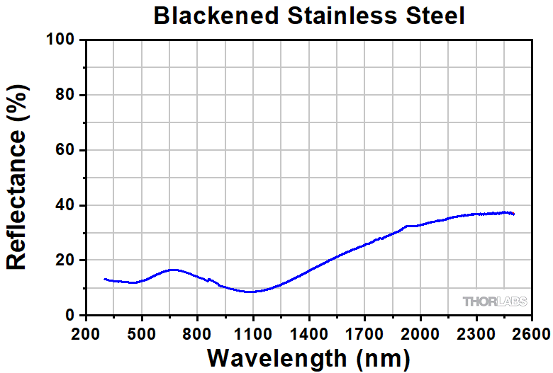
Below is presented a reflectance graph for the blackened stainless steel on the mounted optical slits. The raw reflectance data can be found here.
 Click to Enlarge
Figure 2: Two identical sine waves are shown out-of-phase.
The top two curves are added together in order to get the
resultant in the bottom row. When both waves are
out-of-phase, they interfere destructively.
 Click to Enlarge
Figure 1: Two identical sine waves are shown in-phase. The top two curves are added together in order to get the resultant in the bottom row. When both waves are in-phase, they interfere constructively.
 Click to Enlarge
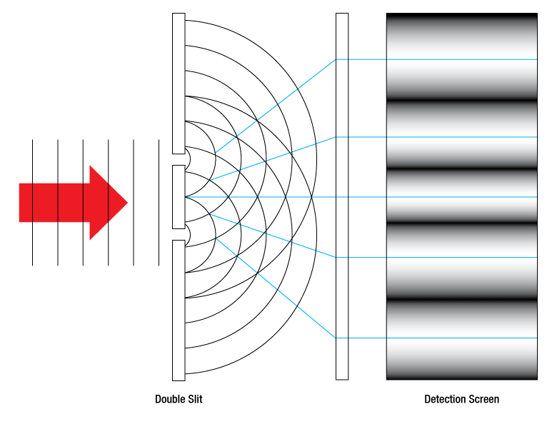
Figure 3: A plane wave is incident on a pair of slits such that each slit acts like a point source that radiates toward a detection screen. The intensity observed on the screen will be an alternating bright and dark pattern due to interference between light from the two slits.
 Click to Enlarge
Figure 4: Two slits are shown separated by a distance d, positioned a distance L from a detection screen. The difference in path length, Δx, from each slit to a particular point y on the screen results in varying levels of constructive and destructive interference.
Click to Enlarge
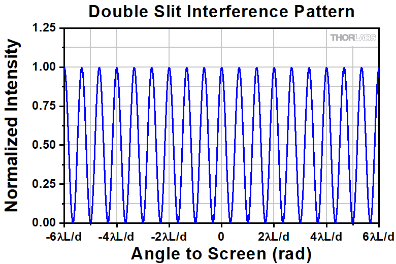
Figure 5: The intensity of light of wavelength λ is plotted at points along a screen which
is a distance L away from a pair of optically small slits that are separated by a distance d.
Click to Enlarge
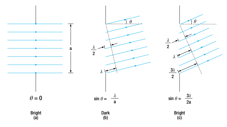
Figure 6: Light of wavelength λ is shown passing through a slit of width a at three
different angles. Case (a) is at an angle of 0°, while cases (b) and (c) are at angles
that result in the first dark fringe and the first non-central maximum, respectively.
 Click to Enlarge
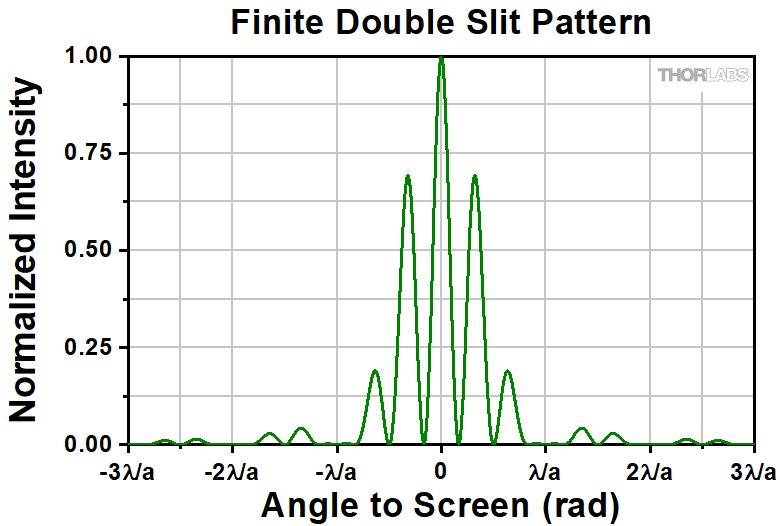
Figure 8: The intensity of light of wavelength λ passing through a pair of slits of width a
which are separated by a distance d=3a is plotted at points along a detection screen at
angles θ away from the horizontal.
 Click to Enlarge
Figure 7: The intensity of light of wavelength λ passing through a slit of width a
is plotted at points along a detection screen at angles θ away from the horizontal.
Double Slit Interference and Diffraction
Constructive and Destructive Interference
Light can be accurately described as both a wave and a particle. The wave-like properties of light determine in what ways light can be manipulated and the phenomena that we can observe. A fundamental property of waves is the principle of superposition, which states that for any number of waves existing in the same space, the observed amplitude at a particular point will be the vector sum of each wave at that position. This phenomenon is easily observed through the concepts of constructive and destructive interference. Consider the two identical sine waves pictured in Figures 1 and 2. To determine how these will interfere, we take the amplitude of each wave at a particular point and add these together. In Figure 1, the two waves are perfectly in phase, so their peaks will be in the same positions. When these identical waves are added together, the result is a wave with the same wavelength, but twice the amplitude; this is known as constructive interference. In Figure 2, the two waves are 180° out of phase with one another; where one wave has a peak, the other will have a trough. Thus, when added together, these waves will effectively cancel out, giving 0 amplitude at every point; this is known as destructive interference.
Young's double slit experiment demonstrates the phenomenon of interference between two light sources and allows us to explore the wave-particle duality of light. To develop the theory behind double slit interference, we will consider two parallel apertures that are significantly smaller than the space between them, d. When a plane wave is incident on a double slit such that the light at each slit is in phase, the light passing through each respective aperture will act as a spherical point source according to Huygens' principle. When observing the light on a screen at a perpendicular distance L away from the double slit plane, we will select a few points of interest to consider. At the point y0 on the screen equidistant between the two slits, since the path length from each source is the same, the light will be in-phase, resulting in constructive interference and a bright spot on the screen. Moving symmetrically up or down from this position, the interfering light will move out of phase as the path lengths begin to differ. Eventually, once the path length difference Δx becomes equal to half of the source wavelength, the light will from each slit will be 180° out of phase, resulting in perfect destructive interference and a dark fringe on the screen. Moving further from the center, we will reach a point where the path lengths differ by another half wavelength, making the light from each source in-phase again. This will then result in constructive interference and another intensity maximum on the screen. These alternating bright and dark fringes make up what is known as a double slit interference pattern, which is shown in Figure 3.
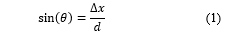
Considering the diagram in Figure 4, we can determine the position y of each bright and dark fringe relative to the center point y0. The relationship between path length difference Δx, slit spacing d, and angle to detection screen θ can be represented trigonometrically as:
Now, the detection angle at which the first intensity minimum (dark fringe) can be found will occur when the path difference is equal to one half of the incident wavelength λ. This angle can also be represented in terms of the perpendicular distance to the screen, L, and the position of the first dark fringe, y, as:

If we now apply the condition that the path length difference will be λ/2 for the first dark fringe, and take advantage of the small angle approximation (for sufficiently small angles, sin(θ) ≅ tan(θ)) we arrive at the result:

Now, to determine subsequent minimum and maximum positions, we can use the same principle; the first non-central bright fringe will occur when the path lengths differ by one full wavelength, λ, and the next dark fringe will occur at the next half-wavelength distance, 3λ/2, etc. Generalizing in terms of an integer m, bright fringes will occur at:
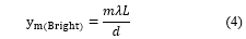
and dark fringes will occur at:
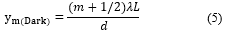
where m is any integer. When m=0, the 0th order maximum will be a distance y=0 away from the central point y0, and the first minimum we found above is known as the 0th order minimum. For a generic case with light of wavelength λ, slit spacing d, and distance L to the screen, this intensity pattern is plotted in Figure 5.
Now, the formulation above assumes that the two slits are infinitesimally small. In reality, the finite size of the slits plays an important role in the resulting intensity pattern. Figure 6 shows a single, finite sized slit of width a with a plane wave incident from a few different angles. By the same principle as the interference discussed above, the range of source positions within the slit will have different path lengths to a detection screen. This leads to a phenomenon known as single slit diffraction. When light passes straight through the slit at θ=0, as in case (a) in Figure 6, each point some distance away from the center of the slit will have an in-phase pair on the opposite side of the slit with which it will interfere constructively at the screen, resulting in a strong central maximum.
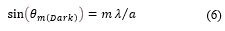
In case (b) where sin(θ)=λ/a, the rays originating at each point in the slit will have a different path length to the same spot; the difference in path length between the top and the bottom of the slit is one full wavelength, while the central point will be out of phase with both by half of a wavelength. We can then consider a point just above the bottom of the slit; similarly to above, there will be a corresponding point that is a/2 above it that will arrive 180° out of phase. In fact, each point in this case will have another with which it interferes destructively, resulting in our first single-slit dark fringe. Similarly to the double slit pattern, for an integer m, the mth order destructive minimum will be found at angles that satisfy the following equation:
Next, considering case (c) where sin(θ)=3λ/2a, the path length for light at the top of the slit will differ from that of the bottom of the slit by 3λ/2. Two thirds of the way down the slit, light will arrive shifted by exactly one wavelength relative to the top of the slit, resulting in constructive interference. Selecting two points slightly below these two will show the same relative phase, such that most rays from this slit will find another with which they interfere constructively, resulting in an intensity maximum. However, unlike the central maximum case, not all rays here will interfere constructively. This results in weaker local maxima on either side of the central bright fringe. Thus, it can be shown that the intensity pattern for light of wavelength λ passing through a single slit of width a will have the following form:
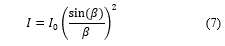
where
which is plotted in Figure 7.
In reality, our double slit is a pair of two finite slits which will both individually undergo diffraction before interfering with each other. Considering cases where the slit spacing d is greater than the slit width a, the positions of the maxima will still be the same as they were for the point-source approximation, ym = mλL/d, but the intensities of each peak are now reduced due to diffraction. To generate the finite-double-slit diffraction pattern, we can just take the product of the theoretical double slit interference pattern and the single slit diffraction pattern. This result for a case where the slit spacing is three times the slit width (as are our double slits with the suffix "K3") is plotted in Figure 8. Generally, the "ideal" double slit intensity pattern will be seen within the diffraction wave packet defined by their individual slit widths.

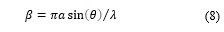
In order to illustrate the process of determining whether a given laser system will damage an optic, a number of example calculations of laser induced damage threshold are given below. For assistance with performing similar calculations, we provide a spreadsheet calculator that can be downloaded by clicking the button to the right. To use the calculator, enter the specified LIDT value of the optic under consideration and the relevant parameters of your laser system in the green boxes. The spreadsheet will then calculate a linear power density for CW and pulsed systems, as well as an energy density value for pulsed systems. These values are used to calculate adjusted, scaled LIDT values for the optics based on accepted scaling laws. This calculator assumes a Gaussian beam profile, so a correction factor must be introduced for other beam shapes (uniform, etc.). The LIDT scaling laws are determined from empirical relationships; their accuracy is not guaranteed. Remember that absorption by optics or coatings can significantly reduce LIDT in some spectral regions. These LIDT values are not valid for ultrashort pulses less than one nanosecond in duration.
A Gaussian beam profile has about twice the maximum intensity of a uniform beam profile.
CW Laser Example
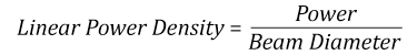
Suppose that a CW laser system at 1319 nm produces a 0.5 W Gaussian beam that has a 1/e2 diameter of 10 mm. A naive calculation of the average linear power density of this beam would yield a value of 0.5 W/cm, given by the total power divided by the beam diameter:
However, the maximum power density of a Gaussian beam is about twice the maximum power density of a uniform beam, as shown in the graph to the right. Therefore, a more accurate determination of the maximum linear power density of the system is 1 W/cm.
An AC127-030-C achromatic doublet lens has a specified CW LIDT of 350 W/cm, as tested at 1550 nm. CW damage threshold values typically scale directly with the wavelength of the laser source, so this yields an adjusted LIDT value:
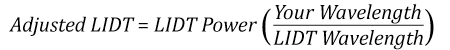
The adjusted LIDT value of 350 W/cm x (1319 nm / 1550 nm) = 298 W/cm is significantly higher than the calculated maximum linear power density of the laser system, so it would be safe to use this doublet lens for this application.
Pulsed Nanosecond Laser Example: Scaling for Different Pulse Durations
Suppose that a pulsed Nd:YAG laser system is frequency tripled to produce a 10 Hz output, consisting of 2 ns output pulses at 355 nm, each with 1 J of energy, in a Gaussian beam with a 1.9 cm beam diameter (1/e2). The average energy density of each pulse is found by dividing the pulse energy by the beam area:
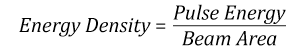
As described above, the maximum energy density of a Gaussian beam is about twice the average energy density. So, the maximum energy density of this beam is ~0.7 J/cm2.
The energy density of the beam can be compared to the LIDT values of 1 J/cm2 and 3.5 J/cm2 for a BB1-E01 broadband dielectric mirror and an NB1-K08 Nd:YAG laser line mirror, respectively. Both of these LIDT values, while measured at 355 nm, were determined with a 10 ns pulsed laser at 10 Hz. Therefore, an adjustment must be applied for the shorter pulse duration of the system under consideration. As described on the previous tab, LIDT values in the nanosecond pulse regime scale with the square root of the laser pulse duration:
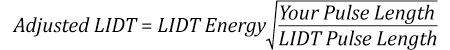
This adjustment factor results in LIDT values of 0.45 J/cm2 for the BB1-E01 broadband mirror and 1.6 J/cm2 for the Nd:YAG laser line mirror, which are to be compared with the 0.7 J/cm2 maximum energy density of the beam. While the broadband mirror would likely be damaged by the laser, the more specialized laser line mirror is appropriate for use with this system.
Pulsed Nanosecond Laser Example: Scaling for Different Wavelengths
Suppose that a pulsed laser system emits 10 ns pulses at 2.5 Hz, each with 100 mJ of energy at 1064 nm in a 16 mm diameter beam (1/e2) that must be attenuated with a neutral density filter. For a Gaussian output, these specifications result in a maximum energy density of 0.1 J/cm2. The damage threshold of an NDUV10A Ø25 mm, OD 1.0, reflective neutral density filter is 0.05 J/cm2 for 10 ns pulses at 355 nm, while the damage threshold of the similar NE10A absorptive filter is 10 J/cm2 for 10 ns pulses at 532 nm. As described on the previous tab, the LIDT value of an optic scales with the square root of the wavelength in the nanosecond pulse regime:
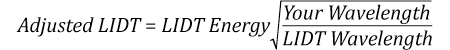
This scaling gives adjusted LIDT values of 0.08 J/cm2 for the reflective filter and 14 J/cm2 for the absorptive filter. In this case, the absorptive filter is the best choice in order to avoid optical damage.
Pulsed Microsecond Laser Example
Consider a laser system that produces 1 µs pulses, each containing 150 µJ of energy at a repetition rate of 50 kHz, resulting in a relatively high duty cycle of 5%. This system falls somewhere between the regimes of CW and pulsed laser induced damage, and could potentially damage an optic by mechanisms associated with either regime. As a result, both CW and pulsed LIDT values must be compared to the properties of the laser system to ensure safe operation.
If this relatively long-pulse laser emits a Gaussian 12.7 mm diameter beam (1/e2) at 980 nm, then the resulting output has a linear power density of 5.9 W/cm and an energy density of 1.2 x 10⁻⁴ J/cm2 per pulse. This can be compared to the LIDT values for a WPQ10E-980 polymer zero-order quarter-wave plate, which are 5 W/cm for CW radiation at 810 nm and 5 J/cm2 for a 10 ns pulse at 810 nm. As before, the CW LIDT of the optic scales linearly with the laser wavelength, resulting in an adjusted CW value of 6 W/cm at 980 nm. On the other hand, the pulsed LIDT scales with the square root of the laser wavelength and the square root of the pulse duration, resulting in an adjusted value of 55 J/cm2 for a 1 µs pulse at 980 nm. The pulsed LIDT of the optic is significantly greater than the energy density of the laser pulse, so individual pulses will not damage the wave plate. However, the large average linear power density of the laser system may cause thermal damage to the optic, much like a high-power CW beam.
| Posted Comments: | |
| No Comments Posted |
| Apertures Selection Guide | |||
|---|---|---|---|
| Aperture Type | Representative Image (Click to Enlarge) |
Description | Aperture Sizes Available from Stocka |
| Single Precision Pinholesa |
 |
Circular Pinholes in Stainless Steel Foils | Ø1 µm to Ø9 mm |
 |
Circular Pinholes in Stainless Steel Foils, Vacuum Compatible |
Ø5 µm to Ø2 mm | |
 |
Circular Pinholes in Gold-Plated Copper Foils | Ø5 µm to Ø2 mm | |
 |
Circular Pinholes in Tungsten Foils | Ø5 µm to Ø2 mm | |
 |
Circular Pinholes in Molybdenum Foils | Ø5 µm to Ø2 mm | |
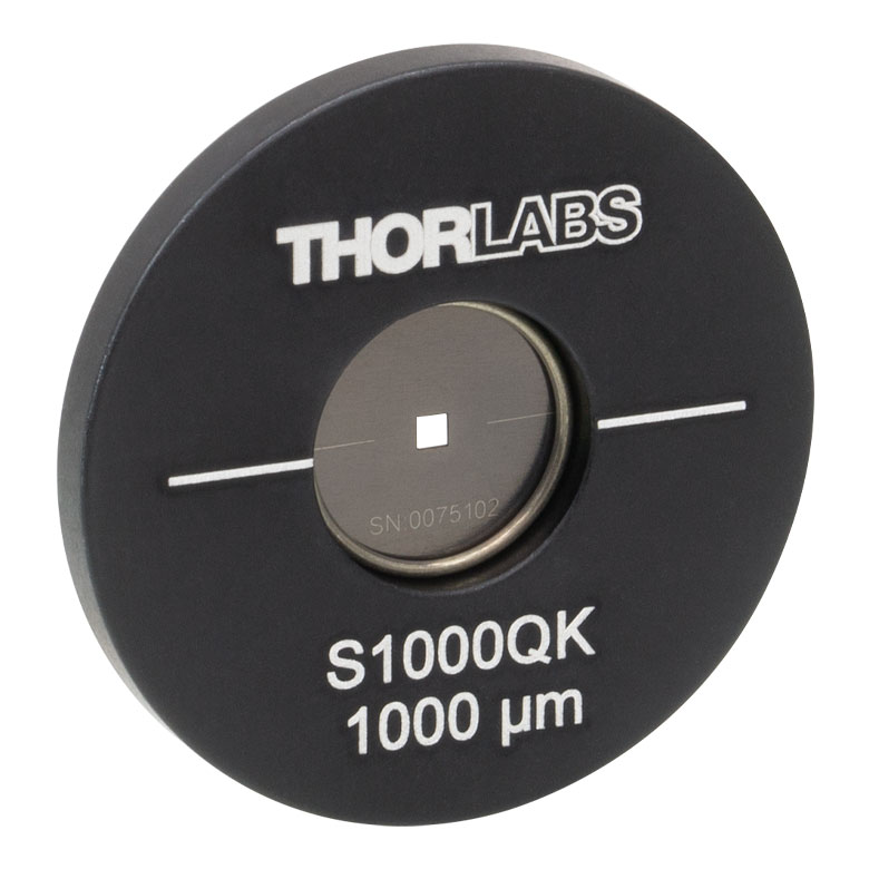 |
Square Pinholes in Stainless Steel Foils | 100 to 1000 µm Square | |
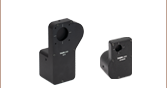
| Slitsa |  |
Slits in Stainless Steel Foils | 3 mm Slit Lengths: 5 to 200 µm Widths 10 mm Slit Lengths: 20 to 200 µm Widths |
 |
Double Slits in Stainless Steel Foils | 3 mm Slit Lengths with 40, 50, or 100 µm Widths, Spacing of 3X or 6X the Slit Width |
|
| Annular Apertures |  |
Annular Aperture Obstruction Targets on Quartz Substrates with Chrome Masks |
Ø1 mm Apertures with ε Ratiosb from 0.05 to 0.85 Ø2 mm Aperture with ε Ratiob of 0.85 |
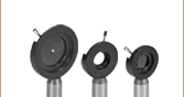
| Pinhole Wheels |  |
Manual, Mounted, Chrome-Plated Fused Silica Disks with Lithographically Etched Pinholes |
Each Disk has 16 Pinholes from Ø25 µm to Ø2 mm and Four Annular Apertures (Ø100 µm Hole, 50 µm Obstruction) |
 |
Motorized Pinhole Wheels with Chrome-Plated Glass Disks with Lithographically Etched Pinholes |
Each Disk has 16 Pinholes from Ø25 µm to Ø2 mm and Four Annular Apertures (Ø100 µm Hole, 50 µm Obstruction) |
|
| Pinhole Kits | 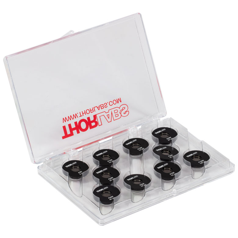 |
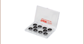
Stainless Steel Precision Pinhole Kits | Kits of Ten Circular Pinholes in Stainless Steel Foils Covering Ø5 µm to Ø9 mm |

 Zoom
Zoom- Optical Slits with Widths of 40, 50, and 100 µm
- Slit Width to Spacing Ratio of 1:3
- 3 mm Slit Length
- Stainless Steel Foils have a Black-Oxide Conversion Coating on Both Sides for Increased Absorbance
These mounted optical slits are available with slit widths of 40, 50, and 100 µm, and spacings of 120, 150, and 300 µm respectively. These slits are fabricated from stainless steel foils that have a black-oxide conversion coating on both sides. The foils are mounted in Ø1", 0.10" (2.5 mm) thick aluminum housings that are black-anodized. The front face of the housings are engraved with the slit item #, slit width, width to spacing ratio, and horizontal lines to aid with slit alignment.
The slits can be taken out of their housings by removing the retaining ring using small tweezers or pliers; use care as the foil is very thin (50 µm).
| Item # | Slit Width | Tolerance | Slit Spacing | Tolerance | Slit Length | Foil Thickness | Foil Diameter | Foil Material | Housing Material |
|---|---|---|---|---|---|---|---|---|---|
| SD40K3 | 40 µm | ±3 µm | 120 µm | ±10 µm | 3 mm | 50 µm | 0.38" (9.6 mm) |
300 Series Stainless Steel, Black-Oxide Conversion Coating |
6061-T6 Aluminum |
| SD50K3 | 50 µm | ±3 µm | 150 µm | ±10 µm | |||||
| SD100K3 | 100 µm | ±4 µm | 300 µm | ±20 µm |

 Zoom
Zoom- Optical Slits with Widths of 40, 50, and 100 µm
- Slit Width to Spacing Ratio of 1:6
- 3 mm Slit Length
- Stainless Steel Foils have a Black-Oxide Conversion Coating on Both Sides for Increased Absorbance
These mounted optical slits are available with slit widths of 40, 50, and 100 µm, and spacings of 240, 300, and 600 µm respectively. These slits are fabricated from stainless steel foils that have a black-oxide conversion coating on both sides. The foils are mounted in Ø1", 0.10" (2.5 mm) thick aluminum housings that are black-anodized. The front face of the housings are engraved with the slit item #, slit width, width to spacing ratio, and horizontal lines to aid with slit alignment.
The slits can be taken out of their housings by removing the retaining ring using small tweezers or pliers; use care as the foil is very thin (50 µm).
| Item # | Slit Width | Tolerance | Slit Spacing | Tolerance | Slit Length | Foil Thickness | Foil Diameter | Foil Material | Housing Material |
|---|---|---|---|---|---|---|---|---|---|
| SD40K6 | 40 µm | ±3 µm | 240 µm | ±20 µm | 3 mm | 50 µm | 0.38" (9.6 mm) |
300 Series Stainless Steel, Black-Oxide Conversion Coating |
6061-T6 Aluminum |
| SD50K6 | 50 µm | ±3 µm | 300 µm | ±20 µm | |||||
| SD100K6 | 100 µm | ±4 µm | 600 µm | ±30 µm |