 Products Home / Technical Resources / Detectors and Power Meters Publications / Photodiodes and Photoconductors Tutorials
Photodiodes and Photoconductors Tutorials

Please Wait

Photodiode Tutorial
Theory of Operation
A junction photodiode is an intrinsic device that behaves similarly to an ordinary signal diode, but it generates a photocurrent when light is absorbed in the depleted region of the junction semiconductor. A photodiode is a fast, highly linear device that exhibits high quantum efficiency and may be used in a variety of different applications.
It is necessary to be able to correctly determine the level of the output current to expect and the responsivity based upon the incident light. Depicted in Figure 1 is a junction photodiode model with basic discrete components to help visualize the main characteristics and gain a better understanding of the operation of Thorlabs' photodiodes.
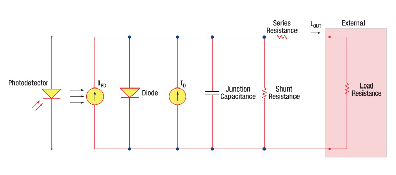
Figure 1: Photodiode Model
Photodiode Terminology
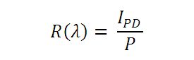
Responsivity
The responsivity of a photodiode can be defined as a ratio of generated photocurrent (IPD) to the incident light power (P) at a given wavelength:
Modes of Operation (Photoconductive vs. Photovoltaic)
A photodiode can be operated in one of two modes: photoconductive (reverse bias) or photovoltaic (zero-bias). Mode selection depends upon the application's speed requirements and the amount of tolerable dark current (leakage current).
Photoconductive
In photoconductive mode, an external reverse bias is applied, which is the basis for our DET series detectors. The current measured through the circuit indicates illumination of the device; the measured output current is linearly proportional to the input optical power. Applying a reverse bias increases the width of the depletion junction producing an increased responsivity with a decrease in junction capacitance and produces a very linear response. Operating under these conditions does tend to produce a larger dark current, but this can be limited based upon the photodiode material. (Note: Our DET detectors are reverse biased and cannot be operated under a forward bias.)
Photovoltaic
In photovoltaic mode the photodiode is zero biased. The flow of current out of the device is restricted and a voltage builds up. This mode of operation exploits the photovoltaic effect, which is the basis for solar cells. The amount of dark current is kept at a minimum when operating in photovoltaic mode.
Dark Current
Dark current is leakage current that flows when a bias voltage is applied to a photodiode. When operating in a photoconductive mode, there tends to be a higher dark current that varies directly with temperature. Dark current approximately doubles for every 10 °C increase in temperature, and shunt resistance tends to double for every 6 °C rise. Of course, applying a higher bias will decrease the junction capacitance but will increase the amount of dark current present.
The dark current present is also affected by the photodiode material and the size of the active area. Silicon devices generally produce low dark current compared to germanium devices which have high dark currents. The table below lists several photodiode materials and their relative dark currents, speeds, sensitivity, and costs.
| Material | Dark Current | Speed | Spectral Range | Cost |
|---|---|---|---|---|
| Silicon (Si) | Low | High Speed | Visible to NIR | Low |
| Germanium (Ge) | High | Low Speed | NIR | Low |
| Gallium Phosphide (GaP) | Low | High Speed | UV to Visible | Moderate |
| Indium Gallium Arsenide (InGaAs) | Low | High Speed | NIR | Moderate |
| Indium Arsenide Antimonide (InAsSb) | High | Low Speed | NIR to MIR | High |
| Extended Range Indium Gallium Arsenide (InGaAs) | High | High Speed | NIR | High |
| Mercury Cadmium Telluride (MCT, HgCdTe) | High | Low Speed | NIR to MIR | High |
Junction Capacitance
Junction capacitance (Cj) is an important property of a photodiode as this can have a profound impact on the photodiode's bandwidth and response. It should be noted that larger diode areas encompass a greater junction volume with increased charge capacity. In a reverse bias application, the depletion width of the junction is increased, thus effectively reducing the junction capacitance and increasing the response speed.
Bandwidth and Response
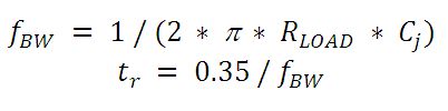
A load resistor will react with the photodetector junction capacitance to limit the bandwidth. For best frequency response, a 50 Ω terminator should be used in conjunction with a 50 Ω coaxial cable. The bandwidth (fBW) and the rise time response (tr) can be approximated using the junction capacitance (Cj) and the load resistance (RLOAD):
Noise Equivalent Power
The noise equivalent power (NEP) is the generated RMS signal voltage generated when the signal to noise ratio is equal to one. This is useful, as the NEP determines the ability of the detector to detect low level light. In general, the NEP increases with the active area of the detector and is given by the following equation:

Here, S/N is the Signal to Noise Ratio, Δf is the Noise Bandwidth, and Incident Energy has units of W/cm2. For more information on NEP, please see Thorlabs' Noise Equivalent Power White Paper.
Terminating Resistance
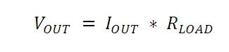
A load resistance is used to convert the generated photocurrent into a voltage (VOUT) for viewing on an oscilloscope:
Depending on the type of the photodiode, load resistance can affect the response speed. For maximum bandwidth, we recommend using a 50 Ω coaxial cable with a 50 Ω terminating resistor at the opposite end of the cable. This will minimize ringing by matching the cable with its characteristic impedance. If bandwidth is not important, you may increase the amount of voltage for a given light level by increasing RLOAD. In an unmatched termination, the length of the coaxial cable can have a profound impact on the response, so it is recommended to keep the cable as short as possible.
Shunt Resistance
Shunt resistance represents the resistance of the zero-biased photodiode junction. An ideal photodiode will have an infinite shunt resistance, but actual values may range from the order of ten Ω to thousands of MΩ and is dependent on the photodiode material. For example, and InGaAs detector has a shunt resistance on the order of 10 MΩ while a Ge detector is in the kΩ range. This can significantly impact the noise current on the photodiode. For most applications, however, the high resistance produces little effect and can be ignored.
Series Resistance
Series resistance is the resistance of the semiconductor material, and this low resistance can generally be ignored. The series resistance arises from the contacts and the wire bonds of the photodiode and is used to mainly determine the linearity of the photodiode under zero bias conditions.
Common Operating Circuits
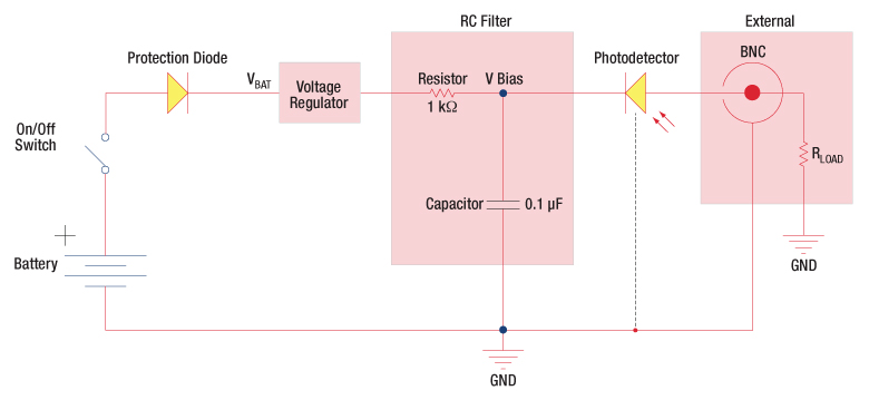
Figure 2: Reverse-Biased Circuit (DET Series Detectors)
The DET series detectors are modeled with the circuit depicted above. The detector is reverse biased to produce a linear response to the applied input light. The amount of photocurrent generated is based upon the incident light and wavelength and can be viewed on an oscilloscope by attaching a load resistance on the output. The function of the RC filter is to filter any high-frequency noise from the input supply that may contribute to a noisy output.
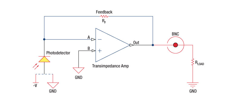
Figure 3: Amplified Detector Circuit
One can also use a photodetector with an amplifier for the purpose of achieving high gain. The user can choose whether to operate in Photovoltaic of Photoconductive modes. There are a few benefits of choosing this active circuit:
- Photovoltaic mode: The circuit is held at zero volts across the photodiode, since point A is held at the same potential as point B by the operational amplifier. This eliminates the possibility of dark current.
- Photoconductive mode: The photodiode is reversed biased, thus improving the bandwidth while lowering the junction capacitance. The gain of the detector is dependent on the feedback element (Rf). The bandwidth of the detector can be calculated using the following:
where GBP is the amplifier gain bandwidth product and CD is the sum of the junction capacitance and amplifier capacitance.
Effects of Chopping Frequency
The photoconductor signal will remain constant up to the time constant response limit. Many detectors, including PbS, PbSe, HgCdTe (MCT), and InAsSb, have a typical 1/f noise spectrum (i.e., the noise decreases as chopping frequency increases), which has a profound impact on the time constant at lower frequencies.
The detector will exhibit lower responsivity at lower chopping frequencies. Frequency response and detectivity are maximized for
![]()
PbS and PbSe Photoconductive Detectors
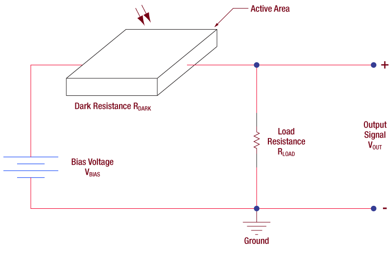
Lead Sulfide (PbS) and Lead Selenide (PbSe) photoconductive detectors are widely used in detection of infrared radiation from 1000 to 4800 nm. Unlike standard photodiodes, which produce a current when exposed to light, the electrical resistance of the photoconductive material is reduced when illuminated with light. Although PbS and PbSe detectors can be used at room temperature, temperature flucturations will affect dark resistance, sensitivity, and response speeds (see Temperature Considerations below).
Click to Enlarge
Theory of Operation
For photoconductive materials, incident light will cause the number of charge carriers in the active area to increase, thus decreasing the resistance of the detector. This change in resistance leads to a change in measured voltage, and hence, photosensitivity is expressed in units of V/W. An example operating circuit is shown to the right. Please note that the circuit depicted is not recommended for practical purposes since low frequency noise will be present.
The detection mechanism is based upon the conductivity of the thin film of the active area. The output signal of the detector with no incident light is defined by the following equation:
![]()
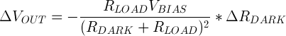
A change ΔVOUT then occurs due to a change ΔRDark in the resistance of the detector when light strikes the active area:
Frequency Response
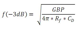
Photoconductors must be used with a pulsed signal to obtain AC signals. Hence, an optical chopper should be employed when using these detectors with CW light. The detector responsivity (Rf) when using a chopper can be calculated using the equation below:
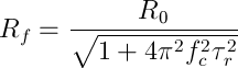
Here, fc is the chopping frequency, R0 is the response at 0 Hz, and τr is the detector rise time.
Effects of Chopping Frequency
The photoconductor signal will remain constant up to the time constant response limit. PbS and PbSe detectors have a typical 1/f noise spectrum (i.e., the noise decreases as chopping frequency increases), which has a profound impact on the time constant at lower frequencies.
The detector will exhibit lower responsivity at lower chopping frequencies. Frequency response and detectivity are maximized for
![]()
See Chapter 5 of the manuals for detector rise time values.
Temperature Considerations
These detectors consist of a thin film on a glass substrate. The effective shape and active area of the photoconductive surface varies considerably based upon the operating conditions, thus changing performance characteristics. Specifically, responsivity of the detector will change based upon the operating temperature.
Temperature characteristics of PbS and PbSe bandgaps have a negative coefficient, so cooling the detector shifts its spectral response range to longer wavelengths. For best results, operate the photodiode in a stable controlled environment.
Typical Photoconductor Amplifier Circuit
Due to the noise characteristic of a photoconductor, it is generally suited for AC coupled operation. The DC noise present with the applied bias will be too great at high bias levels, thus limiting the practicality of the detector. For this reason, IR detectors are normally AC coupled to limit the noise. A pre-amplifier is required to help maintain the stability and provide a large gain for the generated current signal.
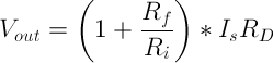
Based on the schematic below, the op-amp will try to maintain point A to the input at B via the use of feedback. The difference between the two input voltages is amplified and provided at the output. It is also important to note the high pass filter that AC couples the input of the amplifier blocks any DC signal. In addition, the resistance of the load resistor (RLOAD) should be equal to the dark resistance of the detector to ensure maximum signal can be acquired. The supply voltage (+V) should be at a level where the SNR is acceptable and near unity. Some applications require higher voltage levels; as a result the noise will increase. The output voltage is derived as the following:
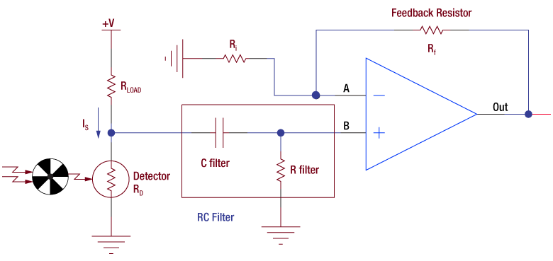
Amplifier Model
Signal to Noise Ratio
Since the detector noise is inversely proportional to the chopping frequency, the noise will be greater at low frequencies. The detector output signal is linear to increased bias voltage, but the noise shows little dependence on the bias at low levels. When a set bias voltage is reached, the detector noise will increase linearly with applied voltage. At high voltage levels, noise tends to increase exponentially, thus degrading the signal to noise ratio (SNR) further. To yield the best SNR, adjust the chopping frequency and bias voltage to an acceptable level.
Noise Equivalent Power
The noise equivalent power (NEP) is the generated RMS signal voltage generated when the signal to noise ratio is equal to one. This is useful, as the NEP determines the ability of the detector to detect low level light. In general, the NEP increases with the active area of the detector and is given by the following equation:
Here, S/N is the Signal to Noise Ratio, Δf is the Noise Bandwidth, and Incident Energy has units of W/cm2.
Dark Resistance
Dark Resistance is the resistance of the detector under no illumination. It is important to note that dark resistance will increase or decrease with temperature. Cooling the device will increase the dark resistance.
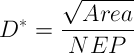
Detectivity (D) and Specific Detectivity (D*)
Detectivity (D) is another criteria used to evaluate the performance of the photodetector. Detectivity is a measure of sensitivity and is the reciprocal of NEP.
![]()
Higher values of detectivity indicate higher sensitivity, making the detector more suitable for detecting low light signals. Detectivity varies with the wavelength of the incident photon.
NEP of a detector depends upon the active area of the detector, which in essence will also affect detectivity. This makes it hard to compare the intrinsic properties of two detectors. To remove the dependence, Specific Detectivity (D*), which is not dependent on detector area, is used to evaluate the performance of the photodetector.
| Posted Comments: | |
| No Comments Posted |