 Products Home / Detectors / Amplified Detectors / InGaAs Amplified Photodetectors / InGaAs Amplified Photodetector with Thermoelectric Cooler
InGaAs Amplified Photodetector with Thermoelectric Cooler

- Sensitive from 0.9 to 2.57 µm
- Built-In TEC Reduces Thermal Noise
- 8-Step Variable Gain and Bandwidth
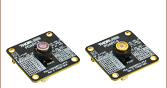
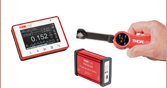
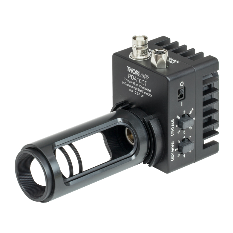
PDA10DT
Post Not Included
Side Mounted
Post Not Included
PDA10DT
Side View,
Post Not Included
Power Supply Included with Detector


Please Wait
| MIR Photodetector Selection Guidea | |||
|---|---|---|---|
| Item # (Detector) | Wavelength Range |
Maximum Bandwidth |
Thermoelectric Cooler |
| PDA10DT (InGaAs) | 0.9 - 2.57 µm | 1,000 kHz | Yes |
| PDA10D2 (InGaAs) | 0.9 - 2.6 µm | 25,000 kHz | No |
| PDA10PT (InAsSb) | 1.0 - 5.8 µm | 1,600 kHz | Yes |
| PDA07P2 (InAsSb) | 2.7 - 5.3 µm | 9 MHz | No |
| PDAVJ8 (HgCdTe) | 2.0 - 8.0 µm | 100 MHz | No |
| PDAVJ10 (HgCdTe) | 2.0 - 10.6 µm | 100 MHz | No |
| PDAVJ5 (HgCdTe) | 2.7 - 5.0 µm | 1 MHz | No |

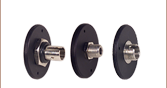
Click to Enlarge
Close-Up of SM1 Threading Around Detector Element
Features
- Sensitive to Mid-IR (MIR) Light from 0.9 - 2.57 µm
- Max Bandwidth of Detector Package: 1 MHz
- Built-In Thermoelectric Cooler Improves Sensitivity
- Ø1 mm Detector Element
- Post Mountable in Two Orientations
- Internally SM1 (1.035"-40) Threaded
- Location-Specific Power Adapter Included
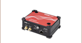
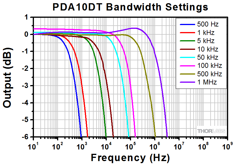
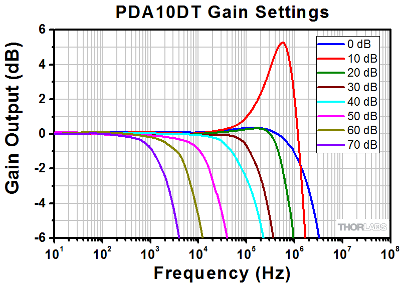
Thorlabs' PDA10DT(-EC) Amplified Detector is a thermoelectrically cooled, photoconductive, extended-range InGaAs (indium gallium arsenide) detector. It is sensitive to light in the mid-IR spectral range from 0.9 to 2.57 µm. Two rotary switches control the gain amplifier and detector package bandwidth, allowing performance to be optimized for a variety of applications. The gain switch features eight discrete steps from 0 - 70 dB, while the bandwidth switch provides eight discrete steps from 500 Hz - 1 MHz. The thermoelectric cooler (TEC) uses a thermistor feedback loop to hold the temperature of the detector element at -10 °C, minimizing thermal contributions to the output signal. For best results, we recommend connecting the BNC output cable (not included) to a 50 Ω termination.
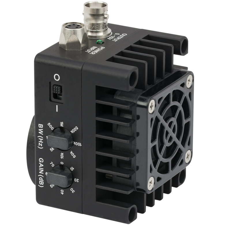
Click to Enlarge
Side View Showing Gain and Bandwidth Adjusters
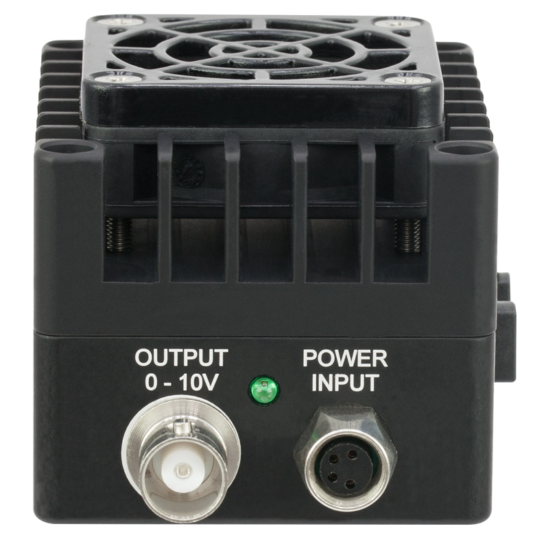
Click to Enlarge
Top View Showing Signal Output and Power Input
The detector package incorporates many of the same mechanical features as our other mounted photodetectors. An internal SM1 (1.035"-40) threading allows Ø1" lens tubes to be mounted in front of the detector element, as shown to the right. Two 8-32 (M4 in the -EC version) tapped holes connect a Ø1/2" post to the housing in one of two perpendicular orientations, as shown in the image at the top of the page. The PDA10DT(-EC) includes a 100 - 240 VAC power adapter. If you require a different adapter plug, please contact Tech Support prior to ordering. An SM1RR Retaining Ring is also included.
Please note that inhomogeneities at the edges of the active area of the detector can generate unwanted capacitance and resistance effects that distort the time-domain response of the output. Thorlabs therefore recommends that the incident light is well centered on the active area. The SM1 (1.035"-40) threading on the housing can be connected to an SM1 lens tube; the lens tube can be used to mount an iris or pinhole in front of the detector element. Because the detector package is flush with the front of the threading, optics and optomechanics cannot be attached directly to the housing.
In addition to the InGaAs detector sold here, Thorlabs manufactures thermoelectrically cooled InAsSb detectors with significantly broader wavelength sensitivity ranges. If a more compact detector housing is desired, we also offer room-temperature amplified photodetectors.
All values given below are for a 50 Ω load, unless otherwise stated.
| Gain (High Z)c | |
|---|---|
| 0 dB | 1.51 x 10³ V/A ± 2% |
| 10 dB | 4.75 x 10³ V/A ± 2% |
| 20 dB | 1.50 x 10⁴ V/A ± 2% |
| 30 dB | 4.75 x 10⁴ V/A ± 2% |
| 40 dB | 1.51 x 10⁵ V/A ± 2% |
| 50 dB | 4.75 x 10⁵ V/A ± 2% |
| 60 dB | 1.50 x 10⁶ V/A ± 2% |
| 70 dB | 4.75 x 10⁶ V/A ± 2% |
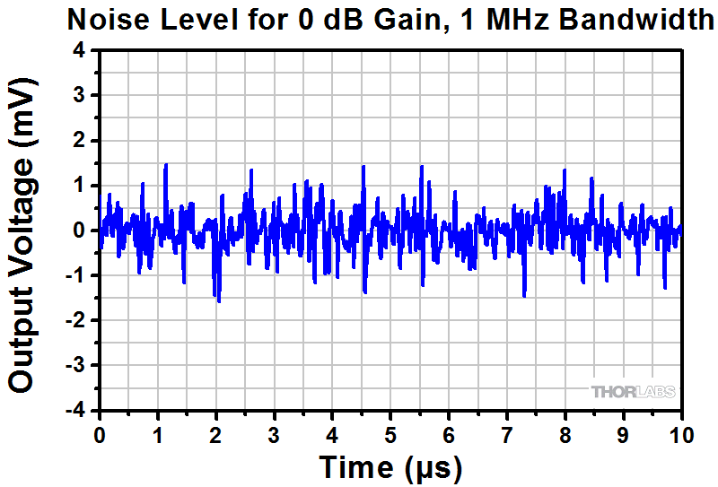
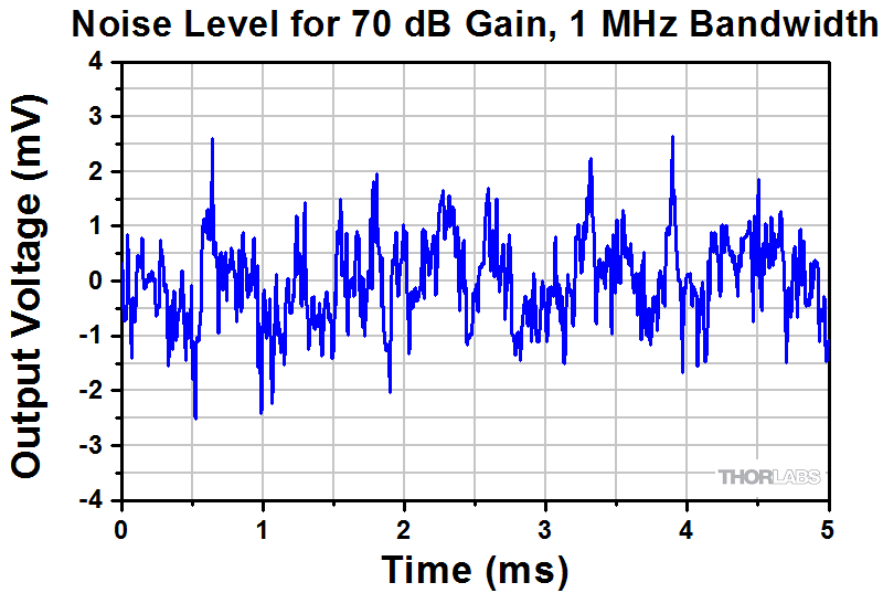
| Noise-Equivalent Power (NEP) Valuesd | |
|---|---|
| 0 dB | 15.9 pW/Hz1/2 @ DC - 2 MHz |
| 10 dB | 8.27 pW/Hz1/2 @ DC - 1.5 MHz |
| 20 dB | 2.8 pW/Hz1/2 @ DC - 700 kHz |
| 30 dB | 1.68 pW/Hz1/2 @ DC - 250 kHz |
| 40 dB | 1.33 pW/Hz1/2 @ DC - 150 kHz |
| 50 dB | 1.88 pW/Hz1/2 @ DC - 20 kHz |
| 60 dB | 2.22 pW/Hz1/2 @ DC - 7 kHz |
| 70 dB | 2.11 pW/Hz1/2 @ DC - 2.5 kHz |
| Item # | PDA10DT(-EC) |
|---|---|
| Optical Specifications | |
| Wavelength Range | 0.9 - 2.57 μm |
| Peak Wavelength (λP) | 2.3 μm |
| Peak Responsivity | 1.3 A/W (Typ.) at Peak Wavelength |
| Electrical Specifications | |
| Gain Settings | 0, 10, 20, 30, 40, 50, 60, or 70 dB (8 Steps) |
| Bandwidth Settings | 0.5, 1, 5, 10, 50, 100, 500, or 1000 kHz (8 Steps) |
| Output Voltagea | 0 - 5 V at 50 Ω 0 - 10 V at High Z |
| Output Impedance | 50 Ω |
| Output Current | 100 mA (Max) |
| Load Impedance | 50 Ω to High Z |
| Output Offsetb | 20 mV (Typ.) 45 mV (Max) |
| Offset Drift | 2.7 mV/°C (at 70 dB Gain) |
| Bias Voltage | -2 V (at 0 dB and 10 dB Gain) 0 V (All Other Gain Settings) |
| Thermoelectric Cooler Specifications | |
| TEC Temperature | -10 °C |
| TEC Current | 0.6 A (Typ.) 0.8 A (Max) |
| Thermistor | 10 kΩ |
| Physical Specifications | |
| Detector Element | Extended Range InGaAs |
| Active Area | 0.8 mm2 (Ø1.0 mm) |
| Surface Depth | 0.08" (2.0 mm) |
| Output | BNC |
| Detector Size | 3" × 2.2" × 2.2" (76.2 mm × 55.9 mm × 55.9 mm) |
| Weight | Detector: 0.42 lbs (191 g) Power Supply: 0.82 lbs (372 g) |
| Power Supply | 30 W, Location-Specific Power Cord Included |
| Input Power | 100 - 120 VAC, 50 - 60 Hz (-EC Version: 220 - 240 VAC) |
| Storage Temperature | 0 to 85 °C |
| Operating Temperature | 0 to 30 °C |
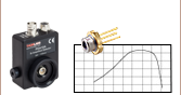
 Click to Enlarge
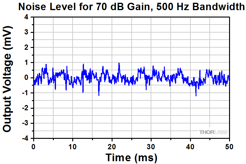
Click to Download Raw Data
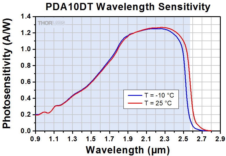
The graph above is for the 0 dB gain setting, and the shaded region denotes the detector's wavelength range.
Output Signal
BNC Female
0 - 5 V at 50 Ω
0 - 10 V at High Z
100 mA Max Current
Power Input
4-Pin Female
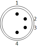
| Pin | Connection |
|---|---|
| 1 | -12 V |
| 2 | Ground |
| 3 | +5 V |
| 4 | +12 V |
The following table lists Thorlabs' selection of photodiodes, photoconductive, and pyroelectric detectors. Item numbers in the same row contain the same detector element.
| Photodetector Cross Reference | ||||||
|---|---|---|---|---|---|---|
| Wavelength | Material | Unmounted Photodiode |
Mounted Photodiode |
Biased Detector |
Amplified Detector |
Amplified Detector, OEM Package |
| 200 - 1100 nm | Si | FDS010 | SM05PD2A SM05PD2B |
DET10A2 | PDA10A2 | - |
| Si | - | SM1PD2A | - | - | - | |
| 240 - 1170 nm | B-Si | - | - | DET20X2 | - | - |
| 320 - 1000 nm | Si | - | - | - | PDA8A2 | - |
| 320 - 1100 nm | Si | FD11A | SM05PD3A | - | PDF10A2 | - |
| Si | - a | - | DET100A2 a | PDA100A2 a | PDAPC2 a | |
| 340 - 1100 nm | Si | FDS10X10 | - | - | - | - |
| 350 - 1100 nm | Si | FDS100 FDS100-CAL b |
SM05PD1A SM05PD1B |
DET36A2 | PDA36A2 | PDAPC1 |
| Si | FDS1010 FDS1010-CAL b |
SM1PD1A SM1PD1B |
- | - | - | |
| 400 - 1000 nm | Si | - | - | - | PDA015A2 FPD310-FS-VIS FPD310-FC-VIS FPD510-FC-VIS FPD510-FS-VIS FPD610-FC-VIS FPD610-FS-VIS |
- |
| 400 - 1100 nm | Si | FDS015 c | - | - | - | - |
| Si | FDS025 c FDS02 d |
- | DET02AFC(/M) DET025AFC(/M) DET025A(/M) DET025AL(/M) |
- | - | |
| 400 - 1700 nm | Si & InGaAs | DSD2 | - | - | - | - |
| 500 - 1700 nm | InGaAs | - | - | DET10N2 | - | - |
| 0.6 - 16 µm | LiTaO3 | - | - | - | PDA13L2e | - |
| 750 - 1650 nm | InGaAs | - | - | - | PDA8GS | - |
| 800 - 1700 nm | InGaAs | FGA015 | - | - | PDA015C2 | - |
| InGaAs | FGA21 FGA21-CAL b |
SM05PD5A | DET20C2 | PDA20C2 PDA20CS2 |
- | |
| InGaAs | FGA01 c FGA01FC d |
- | DET01CFC(/M) | - | - | |
| InGaAs | FDGA05 c | - | - | PDA05CF2 | - | |
| InGaAs | - | - | DET08CFC(/M) DET08C(/M) DET08CL(/M) |
- | - | |
| InGaAs | - | - | - | PDF10C2 | - | |
| 800 - 1800 nm | Ge | FDG03 FDG03-CAL b |
SM05PD6A | DET30B2 | PDA30B2 | - |
| Ge | FDG50 | - | DET50B2 | PDA50B2 | - | |
| Ge | FDG05 | - | - | - | - | |
| 900 - 1700 nm | InGaAs | FGA10 | SM05PD4A | DET10C2 | PDA10CS2 | - |
| 900 - 2600 nm | InGaAs | FD05D | - | DET05D2 | - | - |
| FD10D | - | DET10D2 | PDA10D2 | - | ||
| 950 - 1650 nm | InGaAs | - | - | - | FPD310-FC-NIR FPD310-FS-NIR FPD510-FC-NIR FPD510-FS-NIR FPD610-FC-NIR FPD610-FS-NIR |
- |
| 1.0 - 5.8 µm | InAsSb | - | - | - | PDA10PT(-EC) | - |
| 2.0 - 8.0 µm | HgCdTe (MCT) | VML8T0 VML8T4 f |
- | - | PDAVJ8 | - |
| 2.0 - 10.6 µm | HgCdTe (MCT) | VML10T0 VML10T4 f |
- | - | PDAVJ10 | - |
| 2.7 - 5.0 µm | HgCdTe (MCT) | VL5T0 | - | - | PDAVJ5 | - |
| 2.7 - 5.3 µm | InAsSb | - | - | - | PDA07P2 | - |
Photodiode Tutorial
Theory of Operation
A junction photodiode is an intrinsic device that behaves similarly to an ordinary signal diode, but it generates a photocurrent when light is absorbed in the depleted region of the junction semiconductor. A photodiode is a fast, highly linear device that exhibits high quantum efficiency and may be used in a variety of different applications.
It is necessary to be able to correctly determine the level of the output current to expect and the responsivity based upon the incident light. Depicted in Figure 1 is a junction photodiode model with basic discrete components to help visualize the main characteristics and gain a better understanding of the operation of Thorlabs' photodiodes.
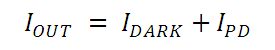
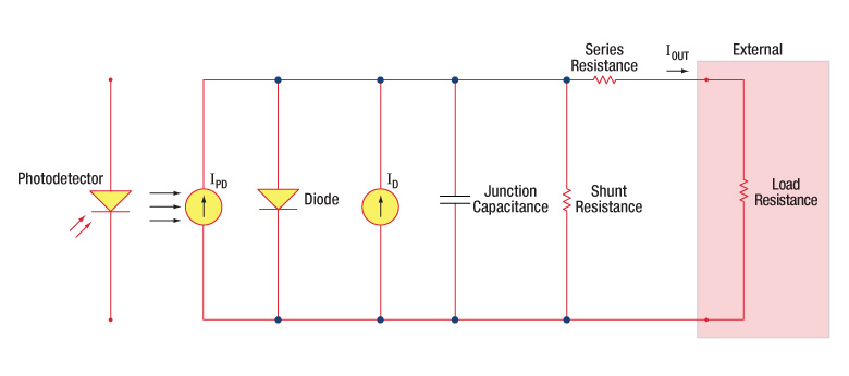
Figure 1: Photodiode Model
Photodiode Terminology
Responsivity
The responsivity of a photodiode can be defined as a ratio of generated photocurrent (IPD) to the incident light power (P) at a given wavelength:
Modes of Operation (Photoconductive vs. Photovoltaic)
A photodiode can be operated in one of two modes: photoconductive (reverse bias) or photovoltaic (zero-bias). Mode selection depends upon the application's speed requirements and the amount of tolerable dark current (leakage current).
Photoconductive
In photoconductive mode, an external reverse bias is applied, which is the basis for our DET series detectors. The current measured through the circuit indicates illumination of the device; the measured output current is linearly proportional to the input optical power. Applying a reverse bias increases the width of the depletion junction producing an increased responsivity with a decrease in junction capacitance and produces a very linear response. Operating under these conditions does tend to produce a larger dark current, but this can be limited based upon the photodiode material. (Note: Our DET detectors are reverse biased and cannot be operated under a forward bias.)
Photovoltaic
In photovoltaic mode the photodiode is zero biased. The flow of current out of the device is restricted and a voltage builds up. This mode of operation exploits the photovoltaic effect, which is the basis for solar cells. The amount of dark current is kept at a minimum when operating in photovoltaic mode.
Dark Current
Dark current is leakage current that flows when a bias voltage is applied to a photodiode. When operating in a photoconductive mode, there tends to be a higher dark current that varies directly with temperature. Dark current approximately doubles for every 10 °C increase in temperature, and shunt resistance tends to double for every 6 °C rise. Of course, applying a higher bias will decrease the junction capacitance but will increase the amount of dark current present.
The dark current present is also affected by the photodiode material and the size of the active area. Silicon devices generally produce low dark current compared to germanium devices which have high dark currents. The table below lists several photodiode materials and their relative dark currents, speeds, sensitivity, and costs.
| Material | Dark Current | Speed | Spectral Range | Cost |
|---|---|---|---|---|
| Silicon (Si) | Low | High Speed | Visible to NIR | Low |
| Germanium (Ge) | High | Low Speed | NIR | Low |
| Gallium Phosphide (GaP) | Low | High Speed | UV to Visible | Moderate |
| Indium Gallium Arsenide (InGaAs) | Low | High Speed | NIR | Moderate |
| Indium Arsenide Antimonide (InAsSb) | High | Low Speed | NIR to MIR | High |
| Extended Range Indium Gallium Arsenide (InGaAs) | High | High Speed | NIR | High |
| Mercury Cadmium Telluride (MCT, HgCdTe) | High | Low Speed | NIR to MIR | High |
Junction Capacitance
Junction capacitance (Cj) is an important property of a photodiode as this can have a profound impact on the photodiode's bandwidth and response. It should be noted that larger diode areas encompass a greater junction volume with increased charge capacity. In a reverse bias application, the depletion width of the junction is increased, thus effectively reducing the junction capacitance and increasing the response speed.
Bandwidth and Response
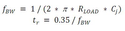
A load resistor will react with the photodetector junction capacitance to limit the bandwidth. For best frequency response, a 50 Ω terminator should be used in conjunction with a 50 Ω coaxial cable. The bandwidth (fBW) and the rise time response (tr) can be approximated using the junction capacitance (Cj) and the load resistance (RLOAD):
Noise Equivalent Power
The noise equivalent power (NEP) is the generated RMS signal voltage generated when the signal to noise ratio is equal to one. This is useful, as the NEP determines the ability of the detector to detect low level light. In general, the NEP increases with the active area of the detector and is given by the following equation:

Here, S/N is the Signal to Noise Ratio, Δf is the Noise Bandwidth, and Incident Energy has units of W/cm2. For more information on NEP, please see Thorlabs' Noise Equivalent Power White Paper.
Terminating Resistance
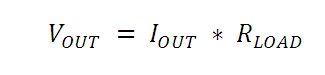
A load resistance is used to convert the generated photocurrent into a voltage (VOUT) for viewing on an oscilloscope:
Depending on the type of the photodiode, load resistance can affect the response speed. For maximum bandwidth, we recommend using a 50 Ω coaxial cable with a 50 Ω terminating resistor at the opposite end of the cable. This will minimize ringing by matching the cable with its characteristic impedance. If bandwidth is not important, you may increase the amount of voltage for a given light level by increasing RLOAD. In an unmatched termination, the length of the coaxial cable can have a profound impact on the response, so it is recommended to keep the cable as short as possible.
Shunt Resistance
Shunt resistance represents the resistance of the zero-biased photodiode junction. An ideal photodiode will have an infinite shunt resistance, but actual values may range from the order of ten Ω to thousands of MΩ and is dependent on the photodiode material. For example, and InGaAs detector has a shunt resistance on the order of 10 MΩ while a Ge detector is in the kΩ range. This can significantly impact the noise current on the photodiode. For most applications, however, the high resistance produces little effect and can be ignored.
Series Resistance
Series resistance is the resistance of the semiconductor material, and this low resistance can generally be ignored. The series resistance arises from the contacts and the wire bonds of the photodiode and is used to mainly determine the linearity of the photodiode under zero bias conditions.
Common Operating Circuits
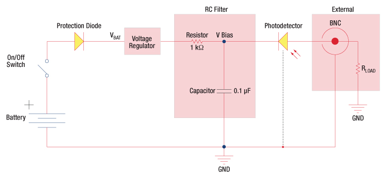
Figure 2: Reverse-Biased Circuit (DET Series Detectors)
The DET series detectors are modeled with the circuit depicted above. The detector is reverse biased to produce a linear response to the applied input light. The amount of photocurrent generated is based upon the incident light and wavelength and can be viewed on an oscilloscope by attaching a load resistance on the output. The function of the RC filter is to filter any high-frequency noise from the input supply that may contribute to a noisy output.
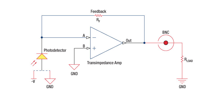
Figure 3: Amplified Detector Circuit
One can also use a photodetector with an amplifier for the purpose of achieving high gain. The user can choose whether to operate in Photovoltaic of Photoconductive modes. There are a few benefits of choosing this active circuit:
- Photovoltaic mode: The circuit is held at zero volts across the photodiode, since point A is held at the same potential as point B by the operational amplifier. This eliminates the possibility of dark current.
- Photoconductive mode: The photodiode is reversed biased, thus improving the bandwidth while lowering the junction capacitance. The gain of the detector is dependent on the feedback element (Rf). The bandwidth of the detector can be calculated using the following:
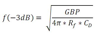
where GBP is the amplifier gain bandwidth product and CD is the sum of the junction capacitance and amplifier capacitance.
Effects of Chopping Frequency
The photoconductor signal will remain constant up to the time constant response limit. Many detectors, including PbS, PbSe, HgCdTe (MCT), and InAsSb, have a typical 1/f noise spectrum (i.e., the noise decreases as chopping frequency increases), which has a profound impact on the time constant at lower frequencies.
The detector will exhibit lower responsivity at lower chopping frequencies. Frequency response and detectivity are maximized for
![]()
| Posted Comments: | |
Ashik A.S
(posted 2021-12-07 07:09:44.84) Hi,
I would like to know what is the maximum input power that can be handled by this detector without damage. There seems to be no specific mention of this in the manual.
-BR
Ashik YLohia
(posted 2021-12-23 12:21:22.0) The saturation/damage threshold is wavelength dependent. Since these devices saturate electrically before they are damaged optically, as long as you are below the output voltage (0-10V), you will not have any chance of damaging this device. alternatively, you can calculate this limit for your own wavelength with the following equation, by simply filling in the appropriate values, as described in section 4.5 of the manual. Hyosub Kim
(posted 2020-09-09 14:12:21.94) Hello, what does -EC stand for?
Is it double sided AR coatings on the borosilicate window? asundararaj
(posted 2020-09-11 10:31:49.0) Thank you for contacting Thorlabs. The -EC in the PDA10DT-EC indicated that the part includes a European power supply, and has metric mounting holes. The PDA10DT comes with a US power supply and has imperial mounting holes. Daan Martens
(posted 2020-07-01 08:38:01.17) We are using PDA10DT-EC in our lab, and similar to earlier posters, we would also very much like this detector with gain that is remote-controllable. asundararaj
(posted 2020-07-02 09:32:17.0) Thank you for your feedback. At the moment, we do not have a PDA with a remote controllable gain and I have logged your request in our internal product forum for future consideration. I have contacted you directly to discuss this further. Sharon Haimov
(posted 2020-05-14 07:01:00.16) Hey,
I'm conduction an experiment, using the trigger-out signal of PDA10DT-EC for another device. i couldn't find any information on the response time (including the photo diode itself and the electronics). could you assist me in that? I want to know the delay/latency/response time of the device.
please send me an email if possible, thanks,
Sharon asundararaj
(posted 2020-05-28 01:53:05.0) Thank you for contacting Thorlabs. We do not have any data or estimates on the delay/latency of the electronics in the PDA10DT-EC. You can estimate the photodiode response from the bandwidth (and gain setting). I have contacted you directly to discuss this further. Rong Zhu
(posted 2020-02-26 14:52:40.4) Do you have similar unit with voltage controllable gain instead of mechanical dial? asundararaj
(posted 2020-02-26 04:42:23.0) Thank you for your feedback. At the moment, we do not have a detector with a voltage controllable gain. I have added this idea to our internal product forum for discussion to offer this at a future time. sergio.vilches
(posted 2019-02-25 15:17:21.4) Dear Thorlabs,
I am analyzing the noise performance of the this sensor and have the following questions:
* The NEP at 70 dB was measured with 1 MHz bandwidth, although the bandwidth of the detector at 70 dB is 2.5 kHz. How meaningful is then the measurement? Could I obtain some details or raw data about the NEP determination?
* Would it be possible to disclose some details about the photodiode you are using? Specifically its dark current, NEP or D*, bandgap, etc
Thanks for your help llamb
(posted 2019-03-08 10:49:08.0) Thank you for your feedback. The 1 MHz bandwidth refers to the highest setting for the low pass filter on the side of the detector's housing. I will reach out to you directly to discuss details of the NEP measurement, as well as the photodiode inside the PDA10DT detector. sergio.vilches
(posted 2018-01-15 16:22:34.13) The Safety Guide provided with the sensor states that it is AC coupled and thus requires a chopped or pulsed source. This is not reflected in the manual. Is there an error then in the Safety guide? tfrisch
(posted 2018-01-16 10:37:49.0) Hello, thank you for contacting Thorlabs. PDA10DT-EC is a DC coupled detector and does not need to be chopped. However, PDA10JT-EC or PDA10PT-EC are both AC coupled detectors that do need to be chopped. I will reach out to you about the Safety Guide you have to clarify this issue. mikita001
(posted 2017-11-22 05:16:03.413) Hi!
Is there a way to order InGaAs Amplified Photodetector with Thermoelectric Cooler PDA10DT with a bigger Active Area? For example 5 mm^2?
Many thanks in advance for your reply!
Best regards,
Mikita tfrisch
(posted 2018-01-17 02:35:38.0) Hello, thank you for contacting Thorlabs. While we don't currently carry a comparable detector with a larger size, I can reach out to you about using a lens to collect light from a larger area. tomaz.rotovnik
(posted 2016-10-05 07:34:02.853) Hello
We are interested for InGaAs Amplified Photodetector with Thermoelectric Cooler to cover ranges from 900nm up to 1700nm. Would be possible to buy Photodetector with calibrated photodiode?
Kind regards
Tomaz jlow
(posted 2016-10-05 10:44:23.0) Response from Jeremy at Thorlabs: Unfortunately we cannot calibrate the PDA10DT because of the small active area. We have other larger area photodetectors that we could calibrate. We will contact you directly to discuss about this. ben.aernouts
(posted 2013-04-23 22:44:09.727) Dear,
We are using a PDA10DT-EC detector in our lab. At 0 dB gain it seems that the dynamic range is smaller compared to other gain settings. With a 50Ω load the dynamic range is 0 - 2.36 Volt and without load, the dynamic range is 0 - 4.7 Volt. For other gain settings it is respectively 0 - 5.15 Volt and 0 - 10.3 Volt.
Increasing the power of the light source when the signal is 2.36 Volt (0 gain, 50Ω load) does not force an increase in the voltage. It seems that the detector is saturated. However, it does not result in a flat line like it is when the detector saturates for other gain settings. There is still some noise on the signal.
Is this normal? What is the reason or cause for this phenomenon? What should we do?
Many thanks and best regards,
Ben Aernouts
Department Biosystems, Division MeBioS
KULeuven
Kasteelpark Arenberg 30, bus 2456
BE-3001 Heverlee
Tel: +32 (0)16 32 14 70
Mobile: +32 (0)4 84 82 50 33
E-mail: Ben.Aernouts@biw.kuleuven.be jlow
(posted 2013-05-02 19:46:00.0) Response from Jeremy at Thorlabs: The PDA10DT-EC should still be outputting a max. of around 10V for Hi-Z load. We will have to take your unit back to evaluate the reason it's not outputting 10V at the 0dB setting. We will get in contact with you on sending your unit back. |
| Item # | PDA10DT(-EC) |
|---|---|
| Click Image to Enlarge | 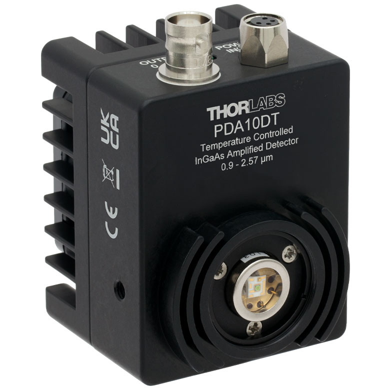 |
| Detector Material (Click for Image) |
Extended Range InGaAs |
| Wavelength Range (λP) | 0.9 - 2.57 µm |
| Peak Wavelength | 2.3 µm |
| Peak Responsivity | 1.3 A/W (Typ.) at Peak Wavelength |
| Active Area | 0.8 mm2 (Ø1.0 mm) |
| Window Material | Borosilicate Glass |
| Gain Settings | 8 Steps: 0, 10, 20, 30, 40, 50, 60, or 70 dB |
| Bandwidth Settings | 8 Steps from 500 Hz to 1 MHz |
| Noise-Equivalent Power (NEP) | 2.11 pW/Hz1/2 @ DC - 2.5 kHz (for 70 dB Gain and 1 MHz Bandwidth) |
- Sensitive to Mid-IR Light from 0.9 µm to 2.57 µm
- Detector is Cooled to -10 °C to Reduce Thermal Noise
- 0.8 mm2 Active Area (Ø1.0 mm)
- Variable Gain Amplifier (1.51 kV/A to 4750 kV/A)
- Variable Bandwidth (500 Hz to 1 MHz)
- Internal SM1 (1.035"-40) Threading
- Location-Specific Power Adapter Included
Click to Enlarge
Click Here to Download Raw Data
The graph above is for the 0 dB gain setting, and the shaded region denotes the detector's wavelength range.